Hey SS gurus!
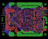
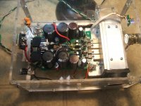
This is my new SS amp module, straight from my mind, aided with some rare aggressive motivation , and is almost complete except for the rest of the PS caps and to finish soldering all the parts in. This is the first proto-type for this module which is a surprise in that I didn’t screw up the first one. I usually at least screw up the first build somehow. Guess this means I must be getting better at this. BTW, I found a company that offered 3 PCBs for $10 each: 2 layers, top/bottom solder mask, and top/bottom silk screen. And they can do 6 mil trace, and 10mil vias! Pretty damn good deal if you ask me.
 My minimum trace is 8mil (just one small place) and minimum via is 12mil.
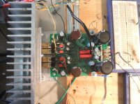
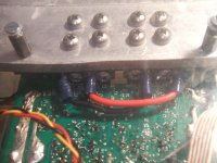
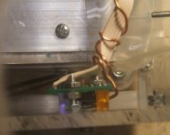
Along with two separate channels, this module features on the PCB, the power supply, both amplifier channels (Av~30dB), control logic with DC detection/protection and clipping detection. The small daughter board mounts onto the front of the enclosure and has a momentary switch and a 3 color LED. The LED is blue for stand-by, green for active, and flashes from green to red for ~0.3 Sec and then back to green if either output is driven into clipping. The logic has DC detection/protection that will activate if either DC output exceeds +/-0.6V, switching the module back into stand-by mode. The heat sink used here is just an old junker.....I'm a fan of using old junk parts.
Instead of using relays to disconnect the speakers from the output stage during power up and power down, it is the output stages that are switched on and off using solid state. This eliminates the relay contacts in series with the speakers. The high current is switched to the output stage circuits by two Mosfets. I chose to use Trench type vertical fets here because of the lower Rds on. These will have two states, either full on or full off. The switching action of off to on state is deliberately slewed to prevent turn on thump, but the turn off action is very fast. There is no sound what so ever when the circuit switches back to stand-by mode. To add another layer of protection, each switched rail is fused. Notice that the voltage regulators do not use Zener diodes for the voltage reference. I detest Zeners used as references in voltage regulator circuits. Zener noise is unnecessary.
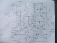
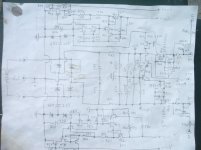
Due to the nature of a public forum, I will discuss the power supply, and the logic control. The output stage circuits are a bit different than what is normally done, but I learned quite a bit from discussions here about the concepts so I will discuss the output stage as well, that is if anybody cares. I chose to use planer stripe type vertical Mosfets for the output stage, they are more suitable for analog applications. The rest is personal IP. Forgive the photos of drawings, I do not have these drawings entered into a computer yet.
Some photos… photo 1, photo 2
This is my new SS amp module, straight from my mind, aided with some rare aggressive motivation
, and is almost complete except for the rest of the PS caps and to finish soldering all the parts in. This is the first proto-type for this module which is a surprise in that I didn’t screw up the first one. I usually at least screw up the first build somehow. Guess this means I must be getting better at this. BTW, I found a company that offered 3 PCBs for $10 each: 2 layers, top/bottom solder mask, and top/bottom silk screen. And they can do 6 mil trace, and 10mil vias! Pretty damn good deal if you ask me. My minimum trace is 8mil (just one small place) and minimum via is 12mil. Along with two separate channels, this module features on the PCB, the power supply, both amplifier channels (Av~30dB), control logic with DC detection/protection and clipping detection. The small daughter board mounts onto the front of the enclosure and has a momentary switch and a 3 color LED. The LED is blue for stand-by, green for active, and flashes from green to red for ~0.3 Sec and then back to green if either output is driven into clipping. The logic has DC detection/protection that will activate if either DC output exceeds +/-0.6V, switching the module back into stand-by mode. The heat sink used here is just an old junker.....I'm a fan of using old junk parts.
Instead of using relays to disconnect the speakers from the output stage during power up and power down, it is the output stages that are switched on and off using solid state. This eliminates the relay contacts in series with the speakers. The high current is switched to the output stage circuits by two Mosfets. I chose to use Trench type vertical fets here because of the lower Rds on. These will have two states, either full on or full off. The switching action of off to on state is deliberately slewed to prevent turn on thump, but the turn off action is very fast. There is no sound what so ever when the circuit switches back to stand-by mode. To add another layer of protection, each switched rail is fused. Notice that the voltage regulators do not use Zener diodes for the voltage reference. I detest Zeners used as references in voltage regulator circuits.
Zener noise is unnecessary.Due to the nature of a public forum, I will discuss the power supply, and the logic control. The output stage circuits are a bit different than what is normally done, but I learned quite a bit from discussions here about the concepts so I will discuss the output stage as well, that is if anybody cares. I chose to use planer stripe type vertical Mosfets for the output stage, they are more suitable for analog applications. The rest is personal IP. Forgive the photos of drawings, I do not have these drawings entered into a computer yet.
Some photos… photo 1, photo 2
Attachments
Last edited:
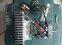
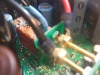
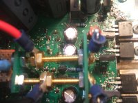
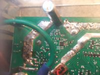
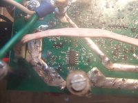
The output transistors are mounted directly to the brass blocks with a screw and HS grease. That brass came from signage scrap, and so being a Gilding metal is 80-90% copper to zinc. It has good thermal properties. The block is energized, energizing the output transistor drain by the tab, and then the drain pin energizes the driving stage and also makes contact with the thermal feedback device. The brass block is insulated from the bracket with mica and grease creating a surface area 4X that of the TO-220 tab, significantly reducing the thermal resistance of the mica layer. Planer stripe mosfets do not have secondary breakdown like characteristics and are limited in Pd by peak die temperature. Also they happen to be cheap, P-ch ~$1.60, N-ch ~$0.69. Most people don't try building a Hi-Fi amp using these devices as source follwer bias in class AB because they are designed for switching and have a nasty exponential transfer, but I believe they are exactly the type of transistor to be driving a reactive load like a speaker. It's all in the gate driving stage. By eliminating the mica pad between the TO-220 tab and the heatsink, the thermal resistance is lowered significantly. The density of the brass block acts as a large thermal capacitor, coupled with little thermal resistance to the transistor die, allows for some abuse. This arrangement creates a thermal filter that reduces the peak temperature spikes. The average temperature is higher but the peak temperature is kept below the point of melt-down, thus I can crank much more power from these output devices. These are rugged devices indeed, each channel can drive at least 80Wrms at 3R! As far as Fairchild Mosfets go, the planer stripe types are denoted with FQ, FQP=TO-220, FQA=TO-247. Obviously the TO-247 components can dissipate more power, but if you notice the datasheets, FQPXXX is the exact same die as FQAXXX. If you can get a more ideal thermal connection to the FQP parts, they will dissipate as much or more power than a FQA part traditionally mounted with mica insulator. The concept with the brass thermal capacitor surprised me with the amount of power that can be sucked through a single pair of TO-220 mosfets.
Mannn, it sounds good. Quite possibly the best amp I've made thus far!!
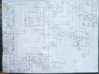
BTW here is the logic circuit...
Going to take a break for a while and listen, but I will post final photos when I get the rest put together....still have to add the Zobels and input filters...
Most people don't try building a Hi-Fi amp using these devices as source follwer bias in class AB because they are designed for switching and have a nasty exponential transfer, but I believe they are exactly the type of transistor to be driving a reactive load like a speaker. It's all in the gate driving stage. By eliminating the mica pad between the TO-220 tab and the heatsink, the thermal resistance is lowered significantly. The density of the brass block acts as a large thermal capacitor, coupled with little thermal resistance to the transistor die, allows for some abuse. This arrangement creates a thermal filter that reduces the peak temperature spikes. The average temperature is higher but the peak temperature is kept below the point of melt-down, thus I can crank much more power from these output devices. These are rugged devices indeed, each channel can drive at least 80Wrms at 3R! As far as Fairchild Mosfets go, the planer stripe types are denoted with FQ, FQP=TO-220, FQA=TO-247. Obviously the TO-247 components can dissipate more power, but if you notice the datasheets, FQPXXX is the exact same die as FQAXXX. If you can get a more ideal thermal connection to the FQP parts, they will dissipate as much or more power than a FQA part traditionally mounted with mica insulator. The concept with the brass thermal capacitor surprised me with the amount of power that can be sucked through a single pair of TO-220 mosfets. Mannn, it sounds good. Quite possibly the best amp I've made thus far!!
BTW here is the logic circuit...
Going to take a break for a while and listen, but I will post final photos when I get the rest put together....still have to add the Zobels and input filters...
Attachments
Last edited:
RushPCB
Click on "3 PCB special". The quality of the PCB is very good. This being the first build of the first prototype, I had to change some SMD components around to fine tune the circuit. It is easy to damage a PCB when removing and replacing SMDs, at least those smaller than 0603.
Click on "3 PCB special". The quality of the PCB is very good. This being the first build of the first prototype, I had to change some SMD components around to fine tune the circuit. It is easy to damage a PCB when removing and replacing SMDs, at least those smaller than 0603.
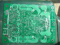
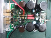
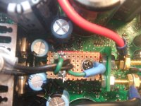
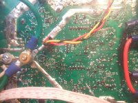
I’m getting closer to being finished with the first build of the first proto-type. The only thing left now is soldering in the final power components and caps, then finding a suitable enclosure. The daughter boards that hold the screws where the speaker wires are attached are mounted in quite solidly. The daughter board closest to the output transistors also have the output Zobel filters and coils. I added the heatsinks for the rectifiers and replaced the temporary fuses with the ones I designed for, 4.5A 0603 SMD. Each channel output stage bias is ~100mA. The small green and yellow wires are just so I can monitor output bias and are just temporary.
I don't see why folks don't use more SMDs. So many components are turning to surface mount. In this circuit I use several varieties of SMD packages. Some of the less common packages for power amp circuits that I used are: SOT-23; SOT-323; SOT723; SOT-923 ; SOT-89; SOT-563; 0603; 0402; and even 0201. 0201 may be small, but the power dissipation is no more than a few mW for these, most are uW. They allow you to cram a lot of circuitry into a small space. Also there are some 0402 resistor arrays. These really save space. This is an advantage in an amplifier circuit. IMHO, power is not needed until you reach the final stages. There are few transistors larger than TO-92 that are even remotely suitable for a VAS. The components in this circuit are not undersized, there was meticulous calculation involved. Don’t think that because the outputs are TO-220 devices that they are not up to the task. I just cranked from one channel about 100Wrms sine wave into 2R resistive and it did not fail
 I think it can handle a reactive 4R speaker with no problem.
I do believe this is the most difficult amp circuit I've conconcted so far. I'm thrilled it was not all for nothing.
Some more pics.
I don't see why folks don't use more SMDs. So many components are turning to surface mount. In this circuit I use several varieties of SMD packages. Some of the less common packages for power amp circuits that I used are: SOT-23; SOT-323; SOT723; SOT-923
; SOT-89; SOT-563; 0603; 0402; and even 0201. 0201 may be small, but the power dissipation is no more than a few mW for these, most are uW. They allow you to cram a lot of circuitry into a small space. Also there are some 0402 resistor arrays. These really save space. This is an advantage in an amplifier circuit. IMHO, power is not needed until you reach the final stages. There are few transistors larger than TO-92 that are even remotely suitable for a VAS. The components in this circuit are not undersized, there was meticulous calculation involved. Don’t think that because the outputs are TO-220 devices that they are not up to the task. I just cranked from one channel about 100Wrms sine wave into 2R resistive and it did not fail I think it can handle a reactive 4R speaker with no problem. I do believe this is the most difficult amp circuit I've conconcted so far. I'm thrilled it was not all for nothing.
Some more pics.
Attachments
Last edited:
1) yes. The voltage drop across the 220R resistor is 6V, set by the current required by the driver and pre-driver/EC. The +/-18V is a bootstrap powered by the output stage, ultamately limited by the zener/diode clamps that prevents overcharging of the gates.
2)No. The input stage is powered from the high voltage rail and +/-40V regulator circuits. When the control circuit is in stand-by, the low voltage high current +/-24V is switched off (B+/B-).
3) the IPS is a complementary J-fet source follower. It is preceeded by a buffer that sums the input signal with the output of the DC servo.
The bootstrap rails lowers the power on the SMT parts. IMO the driver stage should be bias well into class A even if Mosfets are used as outputs. They do require significant gate charge in order to achieve high current slew, even though planer stripe fets are touted as requiring less gate charge per conductance than Hexfets. Although I’m fond of these devices, not everything about planer stripe fets is better than cellular types, they seem to have a greater dependence of Vgs vs. Ic to Vds, an extra distortion but this is nothing the EC can’t deal with. In addition to the bootstrap cascode, there is a traditional cascode. The reason for this is to protect the components used in the EC loop that were chosen to maximize BW. RF devices have very thin base layers and cannot withstand Vce much above 12V. But they can maintain current gain at very high frequencies. I noticed that when the outputs are bias close to class B or cutoff there is a small ~7Mhz oscillation originating from the EC amp, but it disappears when output stage bias approaches 30mA. While oscillation frequencies this high can be hard to track the source, I suspect having bias below this point essentially pushes the PM of the EC amp into instability due to the required increase in voltage gain, or my compensation is too light. (ref principles of HEC) However with bias greater than 30mA (bias is ~100mA), I have not noticed this oscillation. If the EC amp is compensating to this high range of frequencies I suspect the nasty distortions of these 'switching' devices is being nulled to a more than accepta
In addition to the bootstrap cascode, there is a traditional cascode. The reason for this is to protect the components used in the EC loop that were chosen to maximize BW. RF devices have very thin base layers and cannot withstand Vce much above 12V. But they can maintain current gain at very high frequencies. I noticed that when the outputs are bias close to class B or cutoff there is a small ~7Mhz oscillation originating from the EC amp, but it disappears when output stage bias approaches 30mA. While oscillation frequencies this high can be hard to track the source, I suspect having bias below this point essentially pushes the PM of the EC amp into instability due to the required increase in voltage gain, or my compensation is too light. (ref principles of HEC) However with bias greater than 30mA (bias is ~100mA), I have not noticed this oscillation. If the EC amp is compensating to this high range of frequencies I suspect the nasty distortions of these 'switching' devices is being nulled to a more than accepta
Last edited:
very cool indeed, loving the SMD constellation, in one of the photos there is a patch in a slightly out of focus shot that looks like a dirty smudge until you look closely and notice its simply a cloud of tiny SMD. are you hand soldering the o2o4 or have you a home reflow setup? I would be quite interested in building this amp, but I gather by your earlier post that this may not be possible as its to be a fully commercial venture? or just a commercial kit/ready made board?
I too dont quite get the aversion to SMD, to the point folklore would have us believe that its an evil cost cutting exercise, undertaken by faceless men in order to steal our enjoyment of music nevermind the fact that its also higher performance for small signal (and even some large signal) new higher performance parts are designed all the time and almost none will be available in PTH.
i'd love to comment on the input stage and VAS but...... =) intrigued at your results with the TIM
I too dont quite get the aversion to SMD, to the point folklore would have us believe that its an evil cost cutting exercise, undertaken by faceless men in order to steal our enjoyment of music
nevermind the fact that its also higher performance for small signal (and even some large signal) new higher performance parts are designed all the time and almost none will be available in PTH. i'd love to comment on the input stage and VAS but...... =) intrigued at your results with the TIM
This is the first build of the first proto-type, so yes I hand soldered every part including 0201's. The iron I used for this is a 25W iron with a small finishing nail as the soldering tip, along with a tiny flathead screwdriver. Tin one of the pads with solder, then stick the component to the screwdriver tip with solder flux. Place the iron on the pad with the solder and then stick one of the ends of the resistor to the melted solder and adjust the position properly with the screwdriver tip and while holding it in place, remove the iron. Then solder the other side. Those 0402 resistor arrays are not too bad to do either. SOT-923 parts are sort of a pain if the PCB pad layout is not good. You do not want to bury any pads inside large copper spaces because it makes it difficult to heat with a small iron tip. This goes for 0201 parts as well. Learned this the hard way with previous circuits. It is very tedious to do this way, but I plan to try to do a reflow process but I have to get all the component values worked out first. There is a mistake in the PCB that I had to correct for, fortunately it was not a show stopper. I discovered it just after I sent in the Gerber files, and it was too late. There are other minor changes I need to make on the PCB. For a first proto with all that circuitry, it came out pretty good. I would like to eventually make this into a kit, fully assembled but I will need to do a prototype version 2 to get any final bugs worked out of the PCB. I still have 3 PCBs left from this run and enough parts to build 1 more without ordering more, I may try my hand at a reflow trial.
It appears my previous post got cut off some how.
WRT Dimitri's last question, the IPS is cascode complementary common source J-fet with the feedback to the sources ala Borbely. It is preceeded by a buffer that sums the input signal with the output of the DC servo. The VAS is a complementary common gate J-fet stage. It provides 25Vp of signal swing plus the +/-10V spread for the output stage. The VAS bias is controled by a complementary common mode amplifer that modulates the source currents to the IPS.
I used typical miller compensation for the minor loops, and the feedback loop is compensated using TMC. The voltage gain is determined by this loop and also the common mode amplifiers as they too are part of the transfer function, and this is where it gets complex I am slowly but surely working on a paper to provide a better discription of how it works.
The iron I used for this is a 25W iron with a small finishing nail as the soldering tip, along with a tiny flathead screwdriver. Tin one of the pads with solder, then stick the component to the screwdriver tip with solder flux. Place the iron on the pad with the solder and then stick one of the ends of the resistor to the melted solder and adjust the position properly with the screwdriver tip and while holding it in place, remove the iron. Then solder the other side. Those 0402 resistor arrays are not too bad to do either. SOT-923 parts are sort of a pain if the PCB pad layout is not good. You do not want to bury any pads inside large copper spaces because it makes it difficult to heat with a small iron tip. This goes for 0201 parts as well. Learned this the hard way with previous circuits. It is very tedious to do this way, but I plan to try to do a reflow process but I have to get all the component values worked out first. There is a mistake in the PCB that I had to correct for, fortunately it was not a show stopper. I discovered it just after I sent in the Gerber files, and it was too late. There are other minor changes I need to make on the PCB. For a first proto with all that circuitry, it came out pretty good. I would like to eventually make this into a kit, fully assembled but I will need to do a prototype version 2 to get any final bugs worked out of the PCB. I still have 3 PCBs left from this run and enough parts to build 1 more without ordering more, I may try my hand at a reflow trial. It appears my previous post got cut off some how.
WRT Dimitri's last question, the IPS is cascode complementary common source J-fet with the feedback to the sources ala Borbely. It is preceeded by a buffer that sums the input signal with the output of the DC servo. The VAS is a complementary common gate J-fet stage. It provides 25Vp of signal swing plus the +/-10V spread for the output stage. The VAS bias is controled by a complementary common mode amplifer that modulates the source currents to the IPS.
I used typical miller compensation for the minor loops, and the feedback loop is compensated using TMC. The voltage gain is determined by this loop and also the common mode amplifiers as they too are part of the transfer function, and this is where it gets complex
I am slowly but surely working on a paper to provide a better discription of how it works.
Last edited:
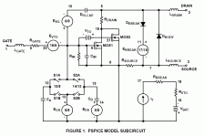
Hi CBS240, could you share your output NMOS model? I used a simplified version of the Fairchild subckt (as shown in the datasheet), by removing the effect of the temperature. It uses a single mosfet (MOSMOD in the model) with a few parameter included into the mosfet and some temperature dependent components removed from subckt. I'm not sure if my model is accurate.
Actually, I'm using P50N06 from Wisdom Semiconductor (WFP50N06). Their datasheet is not complete (so are Fairchilds and other), but the parameters seem to be better than the Fairchild or Intersil ones. I have break the mosfet bodies and it seems Wisdom's are better made.
Actually, I'm using P50N06 from Wisdom Semiconductor (WFP50N06). Their datasheet is not complete (so are Fairchilds and other), but the parameters seem to be better than the Fairchild or Intersil ones. I have break the mosfet bodies and it seems Wisdom's are better made.
Attachments
EDIT
Actually Fairchild mosfet is faster and charge more current, even with higher capacitance. Here is my more simplified model based on Fairchild subckt and PDF:
.model WFP50N06 VDMOS(
+ Rg=0.690 ;RGATE
+ Vto=3.65 ;MOSMOD
+ Rd=10m ;RDRAIN
+ Rs=12m ;RSOURCE
+ Rb=11m ;assumed body diode R = Half Ron
+ Kp=18 ;assumed transconductance param. Fairchild is 35 with twice Qg
+ Cgdmax=1.365n ;PDF max Ciss
+ Cgdmin=1.05n ;PDF typical Ciss
+ Cgs=1.98p ;CIN. why so low
+ Cjo=2.05p ;DBDMOD. why so low
+ Is=1E-30 ;MOSMOD. why so low
+ mfg=Wisdom
+ Vds=60 ;PDF
+ Ron=22m ;PDF
+ Qg=33n) ;PDF
Hi
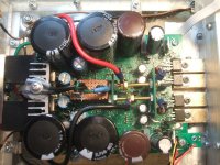
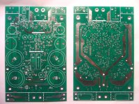
I have completed the next prototype of this unique stereo amplifier module. I lowered the Av to 40 because I usually use the high def audio output card on my laptop as the source so I don’t need much more but it can easily be set up to 60-70 so that an I-pod Nano can be used as the signal source and still clip the output. This PCB is cheap, but is intended to be a prototype. You get what you pay for. If I were to make a production, the PCB would certainly be of better quality. But, this one works for the purpose.
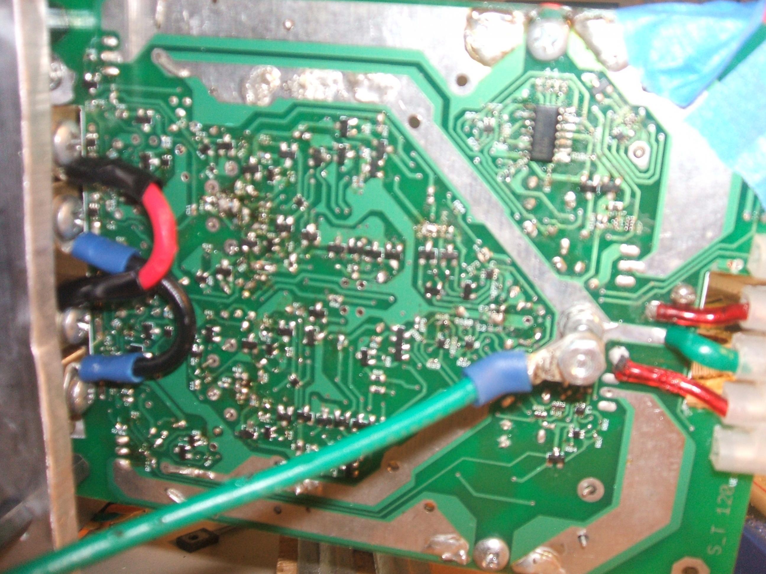
Now I realize many folks don’t like tiny SMD parts and it looks like there is a lot of components crammed onto this PCB, but they each have purpose, from the 0201 size resistors to the large PS caps. There is a lot going on within this PCB than just a couple of amplifiers. In fact most of the circuitry is not part of the amplifiers.
This stereo module is complete with power supply requiring only 18VAC - 0V - 18VAC transformer, voltage doubler & voltage regulator circuits for each amplifier channel’s VAS. It has circuit and speaker protection that is more involved than just a set of relays. The momentary push button switches the amp from stand-by mode (blue) to active mode (green), as indicated by the RGB LED. When the amp is in stand-by, the high current output transistor rails powering the output transistors and gate drive stage are shut off via the two Trench type TO-220 mosfets, the only TO-220 without a heatsink. In this mode, all the brass blocks are de-energized. The output stage for the amplifiers is described in more detail HERE. When the momentary switch is pressed, the LED turns from blue to green and the output stages are energized. There is a delay of about 3 seconds before the relays engage the speakers to the amplifier. The DC detection circuit will be tripped if a DC is output from either channel of more than +/-2.4V for more than about 2 seconds. If for some reason the amp does not settle correctly, the DC output triggers fault before the 3 second delay and the speaker will never engage the amplifier. The switched power rails are fused on both B+ and B- (+/-24V). If either of the fuses break due to a shorted output or any other reason, this is detected and fed back to the control logic resulting in the amp returning to stand-by and will not switch back to active mode. When the amp returns to standby for any reason, there is no delay in the action of the relays.
If you turn up the gain to where the signal begins to clip, then the RGB LED switches from green to red for ~1/3 seconds and then back to green. Nobody likes a clipped signal, so this is a handy indication. The heatsink is a tunnel that I made using some old scrap aluminum signage hardware and a fan is mounted on one side. This fan is controlled by a circuit that senses the heatsink temperature via the small thermistor mounted on the heatsink bracket. The fan is only on when the heatsink becomes hot, but this will not take place unless you are cranking it out so the noise is not an issue. The turn-off limit for the fan is lower than the turn on limit so it will not go --on, off, on, off, ect. The orange LED mounted at the control switch indicates when the fan is running. If for some reason the fan has a fault, and the heatsink gets really hot, the amp will switch back into stand-by mode until the temperature comes down, and then will automatically switch back to active when the temperature returns back below this set point.
The SOT 14 chip on the bottom of the PCB is a TS556 timer chip. The TS is a low current version of a typical 556 timer. The Micro 8 package on the bottom of the PCB is a 339 duel comparator acting as the limit detector for the fan control circuit. There is also a SC 70-5 single comparator and a SC 70-6 D-flip-flop. There are no other IC’s on the board, just tiny TTL, nothing special. The noise floor is so low, I could barely hear a tiny bit of white noise from the tweeter but then my refrigerator in the other room, 30ft away turned on and with that small amount of ambient noise, the white noise is indistinguishable.
Number of transistors? Many
All those tiny SMD’s!!! Here is a list of all the SMD semiconductors used in this circuit:
SOT-14
Micro-8
SC 70-5pin
SC 70-6pin
SOT 89
SOT 23
SOT 323
SOT 723
SOT 923
SOT 563
SOD 923 (diodes)
SOD 523 (diodes)
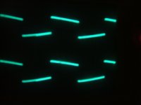
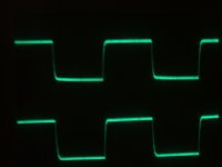
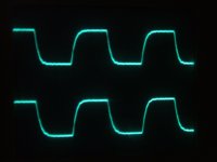
The first waveform photo is 50KHz square wave from each output, 1Vp @ 6R. The second is 10Vp, same load. The third photo is 10KHz square wave, 10Vp. The fourth is 20Hz square wave, 10Vp @ 6R.
I have completed the next prototype of this unique stereo amplifier module. I lowered the Av to 40 because I usually use the high def audio output card on my laptop as the source so I don’t need much more but it can easily be set up to 60-70 so that an I-pod Nano can be used as the signal source and still clip the output. This PCB is cheap, but is intended to be a prototype. You get what you pay for.
If I were to make a production, the PCB would certainly be of better quality. But, this one works for the purpose. Now I realize many folks don’t like tiny SMD parts and it looks like there is a lot of components crammed onto this PCB, but they each have purpose, from the 0201 size resistors to the large PS caps. There is a lot going on within this PCB than just a couple of amplifiers. In fact most of the circuitry is not part of the amplifiers.
This stereo module is complete with power supply requiring only 18VAC - 0V - 18VAC transformer, voltage doubler & voltage regulator circuits for each amplifier channel’s VAS. It has circuit and speaker protection that is more involved than just a set of relays. The momentary push button switches the amp from stand-by mode (blue) to active mode (green), as indicated by the RGB LED. When the amp is in stand-by, the high current output transistor rails powering the output transistors and gate drive stage are shut off via the two Trench type TO-220 mosfets, the only TO-220 without a heatsink. In this mode, all the brass blocks are de-energized. The output stage for the amplifiers is described in more detail HERE. When the momentary switch is pressed, the LED turns from blue to green and the output stages are energized. There is a delay of about 3 seconds before the relays engage the speakers to the amplifier. The DC detection circuit will be tripped if a DC is output from either channel of more than +/-2.4V for more than about 2 seconds. If for some reason the amp does not settle correctly, the DC output triggers fault before the 3 second delay and the speaker will never engage the amplifier. The switched power rails are fused on both B+ and B- (+/-24V). If either of the fuses break due to a shorted output or any other reason, this is detected and fed back to the control logic resulting in the amp returning to stand-by and will not switch back to active mode. When the amp returns to standby for any reason, there is no delay in the action of the relays.
If you turn up the gain to where the signal begins to clip, then the RGB LED switches from green to red for ~1/3 seconds and then back to green. Nobody likes a clipped signal, so this is a handy indication. The heatsink is a tunnel that I made using some old scrap aluminum signage hardware
and a fan is mounted on one side. This fan is controlled by a circuit that senses the heatsink temperature via the small thermistor mounted on the heatsink bracket. The fan is only on when the heatsink becomes hot, but this will not take place unless you are cranking it out so the noise is not an issue. The turn-off limit for the fan is lower than the turn on limit so it will not go --on, off, on, off, ect. The orange LED mounted at the control switch indicates when the fan is running. If for some reason the fan has a fault, and the heatsink gets really hot, the amp will switch back into stand-by mode until the temperature comes down, and then will automatically switch back to active when the temperature returns back below this set point. The SOT 14 chip on the bottom of the PCB is a TS556 timer chip. The TS is a low current version of a typical 556 timer. The Micro 8 package on the bottom of the PCB is a 339 duel comparator acting as the limit detector for the fan control circuit. There is also a SC 70-5 single comparator and a SC 70-6 D-flip-flop. There are no other IC’s on the board, just tiny TTL, nothing special. The noise floor is so low, I could barely hear a tiny bit of white noise from the tweeter but then my refrigerator in the other room, 30ft away turned on and with that small amount of ambient noise, the white noise is indistinguishable.
Number of transistors? Many
All those tiny SMD’s!!! Here is a list of all the SMD semiconductors used in this circuit:
SOT-14
Micro-8
SC 70-5pin
SC 70-6pin
SOT 89
SOT 23
SOT 323
SOT 723
SOT 923
SOT 563
SOD 923 (diodes)
SOD 523 (diodes)
The first waveform photo is 50KHz square wave from each output, 1Vp @ 6R. The second is 10Vp, same load. The third photo is 10KHz square wave, 10Vp. The fourth is 20Hz square wave, 10Vp @ 6R.
Attachments
-
 DSCF7755.JPG265.9 KB · Views: 123
 -
 DSCF7754.JPG253.4 KB · Views: 122
 -
 DSCF7752.JPG291.3 KB · Views: 122
 -
 DSCF7751.JPG286.1 KB · Views: 151
 -
 DSCF7750.JPG326.9 KB · Views: 262
 -
 DSCF7749.JPG290.9 KB · Views: 235
 -
 DSCF7748.JPG186.1 KB · Views: 451
 -
 DSCF7747.JPG180.1 KB · Views: 461
 -
 DSCF7746.JPG193.8 KB · Views: 481
 -
 DSCF7744.JPG193.3 KB · Views: 553
The PCB and some more photos.....
Attachments
-
 DSCF7761.JPG246.3 KB · Views: 67
 -
 DSCF7762.JPG254.5 KB · Views: 65
 -
 DSCF7763.JPG266 KB · Views: 84
 -
 DSCF7764.JPG281 KB · Views: 126
 -
 DSCF7760.JPG271.3 KB · Views: 63
 -
 DSCF7759.JPG278.2 KB · Views: 81
 -
 DSCF7758.JPG343.7 KB · Views: 121
 -
 DSCF7757.JPG343.9 KB · Views: 114
 -
 DSCF7756.JPG311.4 KB · Views: 317
 -
 DSCF7769.JPG342.5 KB · Views: 270
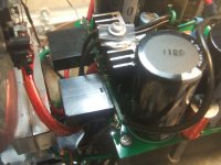
EDIT regarding post 16: The only thing required is the transformer, the voltage doubler ect is all on the PCB.
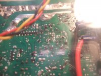
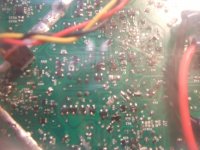
The amplifier stages use a DC servo to set a virtual GND reference for the input transistor so as to zero the output DC. This signal is summed with the audio and fed to a very linear buffer. The audio input capacitors are those red squares under the vero board mounting addition in the center of the PCB. They are 1uf polypropylene film caps from WIMA. These and some small COG type caps used for compensation throughout the amp are the only caps that are directly in the signal path. The IPS and VAS use a common mode differential amplifier, to bias the differential mode amplifier’s common mode current. This common mode error correction scheme seems to allow an enormous linear open loop gain with what seems to be an excellent S/N ratio, when used with the complementary common gate J-fet VAS. While the output Z of this circuit may be quite high, the output stage circuit forms a buffer that only requires a few uA of current to drive. The combination works quite well.
The damping is plenty high enough that it is no problem to drive left and right channels along with left and right rear surround speakers. The output acts more like a voltage source so the effect of the speakers to each other is very minimal if at all. These would be connected in series at opposite phase and placed between the two outputs. Playing only the difference between the left and right channels like this gives you the perception of the sound stage making it very easy to pick out each instrument in the music separately.
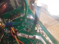
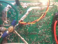
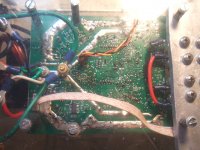
Although it looks fragile with the output wires (the large red and black wires on top) connected to the output node by the screws in the daughter boards. This is quite a sturdy connection. It would take a bit of force to break it. On the final design, I plan to expand the space between the through hole parts just a little bit, but the construction should be quite sound using the proper SMD construction methods of course. Have you ever tried to hand solder 0402 X 4 resistor arrays? Man these are tough!
BTW, despite the perceived size of the output devices (being directly mounted to the brass aides in Pd derating greatly) I can run ~65Wrms @ 4R X 2 channels, plus the surround speakers to full volume. This is plenty for for my home stereo, who wants it much louder than that? I can drive full signal across 2R resistive. The outputs do get warm but didn't fail!
The last photo shows the Zobel filters being close to the output stages. The source ballast resistors are 50mOhm, metal film power resistors from Caddock, TO-126 package.
The amplifier stages use a DC servo to set a virtual GND reference for the input transistor so as to zero the output DC. This signal is summed with the audio and fed to a very linear buffer. The audio input capacitors are those red squares under the vero board mounting addition in the center of the PCB. They are 1uf polypropylene film caps from WIMA. These and some small COG type caps used for compensation throughout the amp are the only caps that are directly in the signal path.
The IPS and VAS use a common mode differential amplifier, to bias the differential mode amplifier’s common mode current. This common mode error correction scheme seems to allow an enormous linear open loop gain with what seems to be an excellent S/N ratio, when used with the complementary common gate J-fet VAS. While the output Z of this circuit may be quite high, the output stage circuit forms a buffer that only requires a few uA of current to drive. The combination works quite well. The damping is plenty high enough that it is no problem to drive left and right channels along with left and right rear surround speakers. The output acts more like a voltage source so the effect of the speakers to each other is very minimal if at all. These would be connected in series at opposite phase and placed between the two outputs. Playing only the difference between the left and right channels like this gives you the perception of the sound stage making it very easy to pick out each instrument in the music separately.
Although it looks fragile with the output wires (the large red and black wires on top) connected to the output node by the screws in the daughter boards. This is quite a sturdy connection. It would take a bit of force to break it. On the final design, I plan to expand the space between the through hole parts just a little bit, but the construction should be quite sound using the proper SMD construction methods of course. Have you ever tried to hand solder 0402 X 4 resistor arrays? Man these are tough!
BTW, despite the perceived size of the output devices (being directly mounted to the brass aides in Pd derating greatly
) I can run ~65Wrms @ 4R X 2 channels, plus the surround speakers to full volume. This is plenty for for my home stereo, who wants it much louder than that? I can drive full signal across 2R resistive. The outputs do get warm but didn't fail!The last photo shows the Zobel filters being close to the output stages. The source ballast resistors are 50mOhm, metal film power resistors from Caddock, TO-126 package.
Attachments
Last edited:
Lots of parts, but it does lots of things. I forgot to mention there is an AC detection circuit that disengages the relays imediately when AC power is switched off eliminating turn off thump.
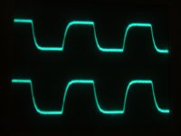
Yes, it seems to be a bit overcompensated. I adjusted the compensation a bit and it is better with the 50KHz square wave, but I think I can get it to be better yet. The top is what it was, and the bottom is now, still a little slew limited. Need to poke and prod some more.
Yes, it seems to be a bit overcompensated. I adjusted the compensation a bit and it is better with the 50KHz square wave, but I think I can get it to be better yet.
The top is what it was, and the bottom is now, still a little slew limited. Need to poke and prod some more.Attachments
- Status
- This old topic is closed. If you want to reopen this topic, contact a moderator using the "Report Post" button.
- Home
- Amplifiers
- Solid State
- New home brew amp module