Hi Guys,
I finally got some time to work on my boards, still no luck. I had to change out R8,9,15,16, & 26. Changed them all to 100R as spec'd in BOM, in the original order Digikey set 100K instead of 100R and I hadn't double checked. I triple checked all of the transistors they are all as called for in the BOM. When power is applied I get 126 VDC across the 10R resistor on F1, and 0.014VDC across the 10R on F2. When I junped the bases of Q14 and Q15 to the end of R43 closest to the bottom of the board, nothing changed. One thing though I checked across each of the legs of the larger transistors for continuity all had now with the excepting of Q13. On Q13 I get 1.16K between the base and the end pin, but no continuity between the base and the middle pin, I don't know enough to know itf this means something.
At this point I'm stumped, I'm beginning to wonder if I got a bunch of bum transistors, or something. Any guidance would be appreciated. I've attached some close up pics.
Thanks
PJN
Attachments
Your VAS heatsink looks like 1/8" stock. That might short out Q11/12.
I just have roof flashing (thin) for this HS and the devices are ideal.
If your meter has the "diode"setting test every device B-E and B-C. On both
of my DMM's ....
Big diodes = .530
small diodes -=.670
small transistors = .7xx (.732 etc.)
Large transistors = .6xx
Remember - red lead to base (or diode anode) for NPN , black lead to
base for PNP.
PS - also check any C-E for a dead short 000-005....I'm doin' this on a Japanese amp now .
.
OS
I just have roof flashing (thin) for this HS and the devices are ideal.
If your meter has the "diode"setting test every device B-E and B-C. On both
of my DMM's ....
Big diodes = .530
small diodes -=.670
small transistors = .7xx (.732 etc.)
Large transistors = .6xx
Remember - red lead to base (or diode anode) for NPN , black lead to
base for PNP.
PS - also check any C-E for a dead short 000-005....I'm doin' this on a Japanese amp now
.OS
Last edited:
Hi Guys,
R25 is fine, the picture makes it look dark I checked it again and it's Ok.
Here are the results of checking things with the diode setting of my DMM
Diode checks :
D1 : 0.005 (looks bad, I checked new spares and they read 0.716)
D2 : 0.005 (bad ?)
D3 : 0.847
D4,5,7, 8 &9 : 0.635 to 0.655
D6 (red led, reads 1.55 and dimly lights up)
D7(blue led, reads 1, doesn’t light up, maybe burnt out, was installed with correct polarity as shown on board)
Transistor checks :
Q 1,2,3,4(NPN) B – C : 0.826 – 0.861, B-E : 0.829 – 0.863, C-E – 1
Q 5 (PNP) B-C : 0.83, B-E : 0.835, C-E : 1.215
Q 6 (PNP) B-C : 0, B-E : 0.756 C-E : 0.754 (looks bad)
Q 7 (NPN) B-C : 0.823, B-E : 0.826, C-E : 1.132
Q 8 (NPN) B-C : 0.76, B-E : 0.279 C-E : 0.915 (B-E very different is this bad ?)
Q 9 (PNP) B-C : 0.815, B-E : 0.821, C-E : 1.89
Q 10 (PNP) B-C : 0.113, B-E : 0.821, C-E : 0.861
Q 11 (NPN) B-C : 0.668, B-E : 0.167, C-E : 0.813(B-E very different is this bad ?)
Q 12 (NPN) B-C : 0.757, B-E : 0.763, C-E : 0.816
Q 13 (NPN) B-C : 0.757, B-E : 0.763, C-E : 0.816
Q 14 (NPN) B-C : 0.757, B-E : 0.763, C-E : 0.816
Q 15 (PNP) I installed the wrong transistor, put a MJE15032 here instead of MJE15033, I screwed up when placing the order. I’ll need to replace this with the correct part.
Q 16,17,18 (NPN) B-C : 0.618, B-E : 0.623, C-E : 1.28
Q 19,20,21 (PNP) B-C : 0.583, B-E : 0.595, C-E : 0.638
So it looks like my mistake with Q15 cost me, D1 & D2 are bad, D7 is burned out, Q6 is bad, Q8 & Q11 look questionable. I’ll replace Q15 and these other parts and give it another try. Thanks for your guidance.
PJN
Hi Guys,
R25 is fine, the picture makes it look dark I checked it again and it's Ok.
Here are the results of checking things with the diode setting of my DMM
Diode checks :
D1 : 0.005 (looks bad, I checked new spares and they read 0.716)
D2 : 0.005 (bad ?)
D3 : 0.847
D4,5,7, 8 &9 : 0.635 to 0.655
D6 (red led, reads 1.55 and dimly lights up)
D7(blue led, reads 1, doesn’t light up, maybe burnt out, was installed with correct polarity as shown on board)
Transistor checks :
Q 1,2,3,4(NPN) B – C : 0.826 – 0.861, B-E : 0.829 – 0.863, C-E – 1
Q 5 (PNP) B-C : 0.83, B-E : 0.835, C-E : 1.215
Q 6 (PNP) B-C : 0, B-E : 0.756 C-E : 0.754 (looks bad)
Q 7 (NPN) B-C : 0.823, B-E : 0.826, C-E : 1.132
Q 8 (NPN) B-C : 0.76, B-E : 0.279 C-E : 0.915 (B-E very different is this bad ?)
Q 9 (PNP) B-C : 0.815, B-E : 0.821, C-E : 1.89
Q 10 (PNP) B-C : 0.113, B-E : 0.821, C-E : 0.861
Q 11 (NPN) B-C : 0.668, B-E : 0.167, C-E : 0.813(B-E very different is this bad ?)
Q 12 (NPN) B-C : 0.757, B-E : 0.763, C-E : 0.816
Q 13 (NPN) B-C : 0.757, B-E : 0.763, C-E : 0.816
Q 14 (NPN) B-C : 0.757, B-E : 0.763, C-E : 0.816
Q 15 (PNP) I installed the wrong transistor, put a MJE15032 here instead of MJE15033, I screwed up when placing the order. I’ll need to replace this with the correct part.
Q 16,17,18 (NPN) B-C : 0.618, B-E : 0.623, C-E : 1.28
Q 19,20,21 (PNP) B-C : 0.583, B-E : 0.595, C-E : 0.638
So it looks like my mistake with Q15 cost me, D1 & D2 are bad, D7 is burned out, Q6 is bad, Q8 & Q11 look questionable. I’ll replace Q15 and these other parts and give it another try. Thanks for your guidance.
PJN
D1,2 = toast
Your blue led is most likely good , DMM does not have enough Voltage
to forward bias it.
By having the wrong driver , you most likely "stressed" the VAS , even if
they are not total "toast" , they might not be reliable long term.
The input stage/cascode run on a separate CRC supply and most likely are
fine.
This is why I run them 68R resistors from the driver emitters to L1 with the outputs disconnected.
Even if I put in a wrong part (I done it , too
), the error would equate to mA's instead of AMP's !!
OS
While I was waiting for spare parts to arrive I thought that I'd study the schematic a bit. It turns out that B &C for Q6 are tied together so that's why the B-C reading was 0 so it looks like Q6 is fine. D1 and D2 are also fine taking a reading across either would just return the value of R4 (5R)because of the way the tracks are laid out. I pulled them off of one board and sure enough once out they tested fine (0.716). I also replaced Q11 which I though might have been bad using the diode test since the B-E diode reading was 0.167, with the new replacement the B-C reading is still 0.167 so it looks like Q11 was fine. this leads me to believe that Q8 is also fine. So for right now I'll just resist the urge to get out my hammer and smash these boards to bits, and just wait calmly for the spare parts for Q15 to come in and give it another try.
PJN
PJN
While I was waiting for spare parts to arrive I thought that I'd study the schematic a bit. It turns out that B &C for Q6 are tied together so that's why the B-C reading was 0 so it looks like Q6 is fine. D1 and D2 are also fine taking a reading across either would just return the value of R4 (5R)because of the way the tracks are laid out. I pulled them off of one board and sure enough once out they tested fine (0.716). I also replaced Q11 which I though might have been bad using the diode test since the B-E diode reading was 0.167, with the new replacement the B-C reading is still 0.167 so it looks like Q11 was fine. this leads me to believe that Q8 is also fine. So for right now I'll just resist the urge to get out my hammer and smash these boards to bits, and just wait calmly for the spare parts for Q15 to come in and give it another try.
PJN
Have patience.
Some semiconductors will be affected by their associated components.
I neglected to tell you that not every one would read the same (B-E,B-C).
I actually simulated the Badger with your reversed (wrong driver). As I suspected ,Q9-10
drew 500ma+ - you most likely blew them... Q11-12 might also be suspect
(Replace your VAS).
The input stage/ cascode/mirror just seemed a little unbalanced , but none
conducted more than a few mA's (fine).
I know it is only simulated , but I have done this before to mirror my
major errors and what Spice predicted as "blown" was indeed "toast"
.OS
Hi Guy's
I'm back again without success, I replaced Q10,Q11,& Q12 in the VAS section (Q10,Q11,Q12), replaced Q15 with the correct one, replaced R8, R9, R15, R16, &R26 with 10R (got 100K mislabled from digikey). Tested all of the transistors with the diode function on my DMM all read fine. Replaced D1 & D2 although it turns out that they were good when I tested them after I removed them. Replaced Q8 which also turned out to be fine when I tested it after it was removed. When I apply power D7 (blue led, (-) rail) now lights and I get very low voltage (0.003) across the 10R resistors across F2. But D6 (red led,(+) rail) does not light up and I read the full rail voltage (62.3 vdc) across the 10R resistor across F1. The resistor across F1 does not get warm. and the DC offset reads -62.3 vdc. I checked all of the transistors on the heat sink and none are grounding out to the sink, and none of the VAS transistors on the little heat sink are grounding out to the little sink. I checked R32 to see if it burned out to prevent currend from lighting up D6 and it's fine and reading 22R, checked D6 and it's also fine. Where should I look from here ? Has anyone else used the ver 2.3 boards ?
Thanks,
PJN
If you read the full rail across the F1-10R , it must be either bad or burning.
From there the V+ goes (past) C12 and to the LED resistor , if anything in the
small signal sections were shorting out this side of R32 , the red led would most likely
light while both R32 AND whatever shorted device "downstream" was burning away.
Still4given's boards had a bad through-hole , my 2.3's did not.
OS
Hi Guy's,
I think I may have found the problem, it appears that I burnt R53 out last time I had powered up. It looks perfect, but when I tested it no good. I replaced it and now I'm getting both D6 and D7 to light up, no voltage across the resistors across F1 and F2, and was able to adjust the DC offset to 0. Looks like I'm in business. By the way I tested all of the inboard jumpers and they all have continuity. Tomorrow I make some time to try and finish things up with the other channel.
Thanks a lot for all of your help,
PJN
patience paid off !
I was about to ask if the resistor was fusible , they don't burn - they just
"cease to exist" . I will use these for R32/33 on my badgers.
Good to hear you didn't break out the hammer.
OS
Hi Guy's,
I think I may have found the problem, it appears that I burnt R53 out last time I had powered up. It looks perfect, but when I tested it no good. I replaced it and now I'm getting both D6 and D7 to light up, no voltage across the resistors across F1 and F2, and was able to adjust the DC offset to 0. Looks like I'm in business. By the way I tested all of the inboard jumpers and they all have continuity. Tomorrow I make some time to try and finish things up with the other channel.
Thanks a lot for all of your help,
PJN
I was about to ask if the resistor was fusible , they don't burn - they just
"cease to exist" . I will use these for R32/33 on my badgers.
Good to hear you didn't break out the hammer.
OS
I still need to put everything together in a fully functioning package so I'm keeping the hammer on standby. But I'm less stressed now and hoping for the best. Stress brings out the dark side which brings out the hammer. When I get it all together I'll post a few pics.
PJN
PJN
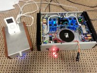
PJN, have patience! This amplifier is sweet! I am amazed by the dynamic impact of the bass, the sound of cymbals/snares (this may have something to do with my ribbon tweeters but it just seems as if they have more presence now), and the L/R channel image is absolutely stunning.
OS, you hit a home run with this one! Thank you for all of your dedication and willingness to share and answer questions about this brilliant design!
Bob, (and everyone else) thank you for answering the few questions I posted...
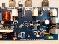
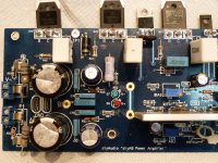
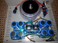
Now, some amplifier porn. I still have to finish designing the front panel and send the design off to be cut. That is, if I can fight off the urge to start my second build the F5t (haven't decided on the variant yet). I think it didn't come out too bad for building this in a hotel room the last few months:
OS, you hit a home run with this one! Thank you for all of your dedication and willingness to share and answer questions about this brilliant design!
Bob, (and everyone else) thank you for answering the few questions I posted...
Now, some amplifier porn. I still have to finish designing the front panel and send the design off to be cut. That is, if I can fight off the urge to start my second build the F5t (haven't decided on the variant yet). I think it didn't come out too bad for building this in a hotel room the last few months:
Attachments
Last edited:
I was taught by others.
Andy C. , GK (discontinued members - brilliant) . Also, this is just a refined version
of Doug Self's "blameless" , which I embraced 4 years ago.
The layout is inspired by the ADCOM 535 1/2 and the study of
100's of Japanese OEM's I've repaired for decades.
With good speakers , this amp will showcase itself. VERY nice build ,
A+++ .
OS
Andy C. , GK (discontinued members - brilliant) . Also, this is just a refined version
of Doug Self's "blameless" , which I embraced 4 years ago.
The layout is inspired by the ADCOM 535 1/2 and the study of
100's of Japanese OEM's I've repaired for decades.
With good speakers , this amp will showcase itself. VERY nice build ,
A+++
.OS
Hi Guys,
I think that I'm just about ready to give this amp another try, but before I make more smoke I'd like to ask a few questions. I powered up each amp separately to make the final adjustments using a light bulb tester. I Adjusted the DC offset to 0, and the small CCS using R7 to get the voltage across R14 to 8.25 vdc as outlined in the build guide. When I began to adjust the bias using R30 once I got much past 20 mV, the filiment on the light bulb tester (60w bulb) began to glow, I set the bias at 44 mV for both amps, and the light bulb glowed equally for each and was pretty bright. Is setting the bias supposed to draw this much current, or am I good to go ?
thanks,
PJN
1/4A+/per rail (60V), that should light the bulbs well. A 60W bulb will draw about .5A @ 120Vac.
If your heatsinks just get warm ,
R37-39= +.63V and R40-42= -.63V (or close) and your output is 0 = bias is good.
PS(edit) - 44mv is a little high (100ma per device) ... won't hurt. 30mv will give 66ma per device. - All
my ON semi models show this as the "sweet spot" for low THD.
Sounds like you got it.
OS
Last edited:
- Home
- Amplifiers
- Solid State
- diyAB Amp The "Honey Badger" build thread