Another remark: If the top is actually where the rough supply enters, you are asking for trouble connecting all grounds to the same plane. How is the rough supply configured? Separate xformer windings, completely isolated, each their own bridge? Then run them isolated to the board, and connect the returns together to the ground plane somewhere centrally where you also can connect feedback returns, reference returns etc.
Jan Didden
Jan Didden
I think it's a good idea (as most application notes suggest) that you connect the digital and analog ground somewhere near (under?) the DAC. Also I agree with Jan, try to place the DAC in the center so you will have as much as possible of groundplane.janneman said:Then run them isolated to the board, and connect the returns together to the ground plane somewhere centrally where you also can connect feedback returns, reference returns etc.
Why don't you change the opamps to SO08 or at least have both? (Sorry Fred!)
peranders said:You have 1206 or 0805 (can't see) and equally fat traces as the pads. This can be troublesome if you solder by hand. Sometimes you must have "hot relief" pads. This can be fixed with a fat main trace and them a 15 mil trace to the pad. Make this trace not too long (max 1-2 mm). The HF guys don't like it.
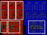
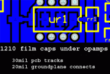
They are 1206 resistors, and 1210 film caps. I currently have 20mil relief connects from the ground plane to the components. I will work on making the traces on the other side thinner. Is 20 mil fine on the ground plane connect lines to the components?
peranders said:BTW: Shouldn't you use separate ground planes for the analogue and and digital section?
Yes, there will be seperate ground planes. The board will essentially be twice as wide, as I haven't added the digital side to the pcb layout yet. (left of the dac chip, will be digital ground plane and circuitry).
Fred Dieckmann said:
Good advice, Brian. I see you have them on the pads into the ground plane. We call them thermal spokes where I worked. Even when oven soldering SMT parts will pull toward the larger thermal mass.
Is 20mil to large for the "thermal spokes" from the ground plane? I will add thinner connections from the main lines to the pads for easier soldering.
As for the trace width, do I really need 60mil traces on the power supply lines, or can I scale them down more? Would the higher impedence of using 40mil traces instead of 60mil really effect the design, or the lower current handling cause problems?
--
Brian
janneman said:Another remark: If the top is actually where the rough supply enters, you are asking for trouble connecting all grounds to the same plane. How is the rough supply configured? Separate xformer windings, completely isolated, each their own bridge? Then run them isolated to the board, and connect the returns together to the ground plane somewhere centrally where you also can connect feedback returns, reference returns etc.
I was planning on making a seperate power supply pcb, regulating the voltages before sending them into the pre-reg on the pcb. I am planning on having seperate windings, bridges, capacitor banks, and regulators, but haven't decided how to run the grounding. You mention isolated to the board. Is this implying that I don't tie the ground on the power supply pcb to the central ground, but just run the voltage and ground to the pcb, which is in turn tied to the central ground. What exactly is implied by feedback returns and reference returns? I was just looking at running one line for voltage, and one ground line for each on-board regulator. Is this wrong?
peranders said:
I think it's a good idea (as most application notes suggest) that you connect the digital and analog ground somewhere near (under?) the DAC. Also I agree with Jan, try to place the DAC in the center so you will have as much as possible of groundplane.
Why don't you change the opamps to SO08 or at least have both? (Sorry Fred!)
hmm.. under the dac is the best place to run a single trace connecting digital and analog ground?
As for the opamps, I wanted the option of using a wider array of opamps, and being able to swap them out initially with sockets (sockets can be removed when the desired opamp is chosen. I used through-hole components also for the opamps, as I would have had to run a good amount of vias anyway, given the way I wanted to run power.
--
Brian
Brian, it's easier than you think. DIL08 serves also as via holes. Just place an SO08 between the pad row of DIL08.BrianGT said:As for the opamps, I wanted the option of using a wider array of opamps, and being able to swap them out initially with sockets (sockets can be removed when the desired opamp is chosen. I used through-hole components also for the opamps, as I would have had to run a good amount of vias anyway, given the way I wanted to run power.
I recommend 15 mils hot releif bars, 2 or 4 pcs. at each ground pad and a single 15 mils for the other ones.
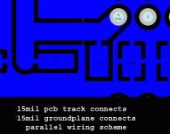
Here is my current scheme:
should I move to thinner traces still? Will this be impossible to solder if left this way?
should I run main v+ trace -> electrolytic -> film -> opamp, or another way? Should I run a trace from the main trace for each?(parallel arrangement)
EDIT: i didn't see per-anders post above when i posted this. anyone else have an opinion as well?
--
Brian
Attachments
grataku said:Brian,
I must say you are becoming quite good with the layouts. That's an impressive board.
Thanks, but I am still quite a beginner, and have learned a lot from others suggestions. I appreciate all the input from others for this.
--
Brian
Brian, I don't know if you believe or not but in case you don't, just etch a test pcb and test this. The thing is cooling, too fast. You what happens when the tin cools off too fast -> ugly and sometimes bad solder joints.
The last attemt looks just about what I suggested.
Just in case: Put in a capacitor after the output resistor. This for preventing EMI to slipping out. The frequency can be rather high 100 kHz or more. You have good possibilities to filter at the pcb with SMD parts. Maybe 100 (or more) pF NPO can be a good start.
peranders said:Brian, I don't know if you believe or not but in case you don't, just etch a test pcb and test this. The thing is cooling, too fast. You what happens when the tin cools off too fast -> ugly and sometimes bad solder joints.
The last attemt looks just about what I suggested.
Just in case: Put in a capacitor after the output resistor. This for preventing EMI to slipping out. The frequency can be rather high 100 kHz or more. You have good possibilities to filter at the pcb with SMD parts. Maybe 100 (or more) pF NPO can be a good start.
Would I really want to put a ceramic capacitor in there? Is that alright?
--
Brian
This capacitors should work from 100 kHz and GOOD to above 500 MHz in order to filter good. NP0 has rather good charactersistics. Values is 1 nF (uncommon) to 100 pF depending of demands. You should also think about the frequency properties from the DAC output and forward.BrianGT said:Would I really want to put a ceramic capacitor in there? Is that alright?
Not this capacitor is optional but have it mind. The I/V converter and the following stage is sensitive when it comes to component choices.
Re: Re:See also
Hi,
Here is a picture of my low noise supply for phonostage or preamp.
Center row IC's from bottem to top: LT1021-5 reference, OP27 low-pass filter, OP07 +5V to -5V converter. BD139/BD140 on coolers. OP27's next to coolers. AD797 can also be used.
")
It's all from datasheets (REF02, OP176)
Elso Kwak said:
See also this paper by Hank Zumbahlen of Analog Devices:
http://www.analog.com/UploadedFiles/Application_Notes/14452667AN394.pdf
Fig. 26 on page 11.
Hi,
Here is a picture of my low noise supply for phonostage or preamp.
Center row IC's from bottem to top: LT1021-5 reference, OP27 low-pass filter, OP07 +5V to -5V converter. BD139/BD140 on coolers. OP27's next to coolers. AD797 can also be used.
It's all from datasheets (REF02, OP176)
Attachments
Black Stuf
Hi Troels,
Phonostage: balanced head amp and phono with RIAA correction.
You want to see it?
tbla said:whats all the black at the right.......
Hi Troels,
Phonostage: balanced head amp and phono with RIAA correction.
You want to see it?
- Status
- This old topic is closed. If you want to reopen this topic, contact a moderator using the "Report Post" button.
- Home
- Amplifiers
- Solid State
- another jung super regulator pcb layout