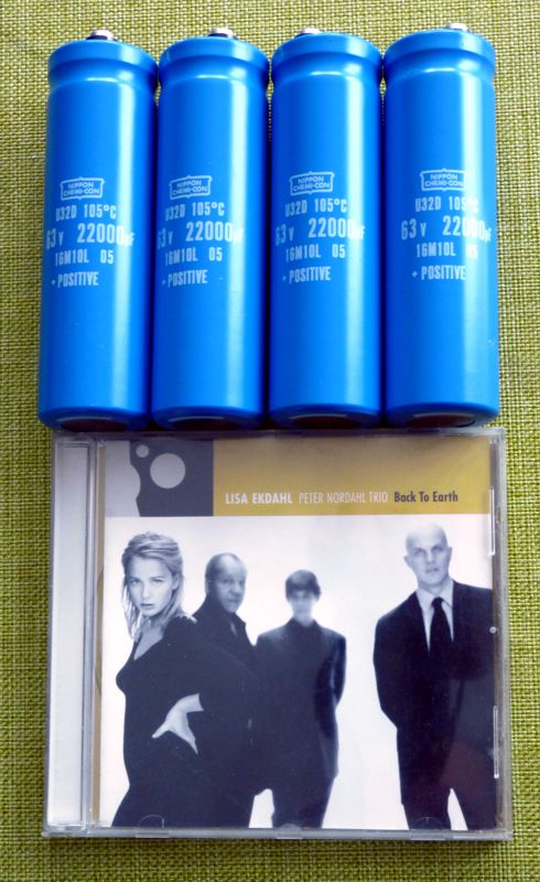
Will you use 88.000 uF for one channel?
I have allready 4u 22.000uf 63V U32D chemicon nipon (diam 35mm L=115mm) and wanted to had a another set. The goal is to be abble if it's possible to drive for domestical use some 3ohms speaker (2.5way speakers for exemple or 2 way speakers with two woffer in parallel)
EPCOS - B57703M103G40 - NTC Thermistor
The last one puts everything in a new perspective regarding NTC PCB installation, it can be mounted and soldered the same way as IRFs, no need for two extra pins.
That's the way to go.
Past few day i ask you a little question about BIGBT BJT selection
I take a look at NJW3281G/1302G datatsheet. They seems to good candidat for job as NPN/PNP gain matching is giving in 10%, that let good matching previsions between NPN and PNP after HFE/Vbe mesuring session.
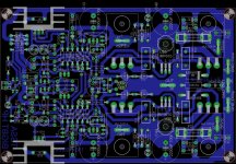
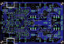
For layout I need to rework to see if i can gain space et reducing traks length, but i am in single layer....that not easy. Pearhaps i can do something with TSSA core to bring it back, more closely to BIGBT module.
Marc
The next things is to fix the IRF610/9610 driver selection.....think diy-beginner will ask question.......not only me.....
Marc
Last edited:
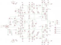
Do R3 & R36 need to be so low?
What deteriorates if 100k and 1k are adopted?
What values are C1 & C2?
2.2mF or 22mF.
I can't make out a decimal point. I prefer 2m2F instead of 2.2mF. It is unambiguous and generally recognised worldwide.
Reported to component voltage value and size this are 2m2uf or 2200uF if you prefer. Same 1mf = 1000uF
Marc
I know and you know that m is short for milli and that m is generally accepted to be the multiplier, 10^-3
But that is not what I am asking.
It's the near invisibility of a decimal point that is causing the ambiguity.
Use 2m2F to avoid 2.2mF being mistaken for 22mF.
Now back to the question: what are the values for C1 & C2? 2m2uF, what the **** is that?
But that is not what I am asking.
It's the near invisibility of a decimal point that is causing the ambiguity.
Use 2m2F to avoid 2.2mF being mistaken for 22mF.
Now back to the question: what are the values for C1 & C2? 2m2uF, what the **** is that?
Last edited:
I think the question is whether or not to avoid irf9xxx due to the way IRF make their P channel mosFETs...........The next things is to fix the IRF610/9610 driver selection.....think diy-beginner will ask question.......
What about Fairchild, or any of many others, who/that seem to have avoided this manufacturing characteristic (or is it a defect that is tolerable in switching applications).
I know and you know that m is short for milli and that m is generally accepted to be the multiplier, 10^-3
But that is not what I am asking.
It's the near invisibility of a decimal point that is causing the ambiguity.
Use 2m2F to avoid 2.2mF being mistaken for 22mF.
Now back to the question: what are the values for C1 & C2? 2m2uF, what the **** is that?
I understand andrew and apply what you suggest(see under). For your value proposal let LC answer...
Marc
Attachments

f=femto
F=Farad
correct that mistake.
the multiplier is used instead of the decimal point.
2m2F is different from 2mf2 and is different from 2mF2
I see 0R22 elsewhere. Good, no confusion.
So no confusion possible, no?
Attachments
I know and you know that m is short for milli and that m is generally accepted to be the multiplier, 10^-3
But that is not what I am asking.
It's the near invisibility of a decimal point that is causing the ambiguity.
Use 2m2F to avoid 2.2mF being mistaken for 22mF.
Now back to the question: what are the values for C1 & C2? 2m2uF, what the **** is that?
Hi AndrewT
Look here's the original schematic, where you can clearly see 2,2 mF. This sort of value marking occupies less space on a schematic than 2.200 μF
Last edited:
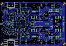
Here we go, R1/C1 value are these from SSA schematic form moment until value is fixed. The add of latest component don't let keep the nice input area symetry we had in previous version.
Marc
Good, good Marc, I like it a lot
Last corrections from me and than I rest my case, PCB can be final:
- C17 100 pF, put three pads/holes as with C8, C9 (5 mm, 7,5 mm)
- move input connector J10 to the middle (symmetry line) and resistor R3 near R36, in that way both connectors J3 and J10 will be aligned
- move two NTC pads closer to R24, and make a screw access hole larger
- J9, J8 are not the same distance away from J5, please correct it
- if possible leave the body of IRFs on the same spot, only align their pads with MJLs, if parts library allows that modification. It would be nice to have pins aligned, also pin leads of IRFs would be shoter (this is the main reason), but please do not move the cases of IRFs
- C12, C15, C41, C42, C43, C45, C46, C47 1 uF film capacitors should have third pad for 5 mm pin distance case, which are quite common on the market
Regards Andrej
P.S. Other answers will follow at the evening
Last edited:
less than 2m2F? and less ambiguously when the decimal point cannot be seen?the original schematic, where you can clearly see 2,2 mF. This sort of value marking occupies less space on a schematic than 2.200 μF
I cannot understand why anyone would want to write 1000uF instead of 1mF, nor 100000uF instead of 100mF, nor 0.0000027uF instead of 2p7F, even 0.0027nF would be a nonsense.
Farad is the basic unit, all others are Farads and a multiplier. Choose the multiplier that best suits the value being displayed, but overall, make it unambiguous.
BTW,
means 2u2F to me and others who understand the decimal point usage.2.200 μF
Last edited:
Good, good Marc, I like it a lot
Last corrections from me and than I rest my case, PCB can be final:
- C17 100 pF, put three pads/holes as with C8, C9 (5 mm, 7,5 mm)
- move input connector J10 to the middle (symmetry line) and resistor R3 near R36, in that way both connectors J3 and J10 will be aligned
- move two NTC pads closer to R24, and make a screw access hole larger
- J9, J8 are not the same distance away from J5, please correct it
- if possible leave the body of IRFs on the same spot, only align their pads with MJLs, if parts library allows that modification. It would be nice to have pins aligned, also pin leads of IRFs would be shoter (this is the main reason), but please do not move the cases of IRFs
- C12, C15, C41, C42, C43, C45, C46, C47 1 uF film capacitors should have third pad for 5 mm pin distance case, which are quite common on the market
Regards Andrej
P.S. Other answers will follow at the evening
Here for update
Marc
Attachments
Last edited:
Mark awesome
Only one little beauty remark hehe, look C8 and C15, what is the difference? Something about silk screen layer and this artefact should be corrected all over the PCB.
For you Sir...
Attachments

Hehe you corrected C15 but at the same time something happened with C8. At other places too.
this time i don't see, all symetrical above from down to top????
marc
C17, C8, C9, C44, C47, C56 capacitor symbol over the pad
Okayyyyyyy....
Marc

Here....One thing is clear, TTSA layout was really rewarding for me. Thanks for all.
I believe that Marc.
C17

Attachments
Last edited:
- Home
- Amplifiers
- Solid State
- TSSA - The Simplest Symmetrical Amplifier