So if we don't want auto protection extra circuits maybe it can be done to switch manually the delay thing, or double it as a remote main bias ''on'' from standby, using a far away preamp?
TLP accepts the same signal (delay-on from protection circuit) as there would be mechanical relay on a PCB.
+ 12 V trigger signals from preamp or HT system via remote connector, turn on power supply's soft-start circuit, which is the different thing. Trigger signal puts on the whole amp from stand-by mode to on mode. After that sequence is done and if everything is OK, protection circuit sends internal 12 V remote signal to amp's PCB to turn output power transistors on.
")
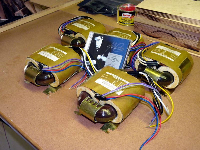
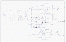
I think i have enough transformers (500Va 2x36Vac) for dual mono .... take a look picture under
Don't know what futur is made from so i think to had 2x10000µf per board.
I have been waiting for modification
Marc

Transformers are super duper ones
 now you can make it as dual mono power amp.
I hope the sch mods can be implemented to existing PCB.

Hi LC i take note from you modification a will work today later on for routing
This systeme seems quite interesting could you details more.
Marc
Hi Salas
No, TLP627 serves to switch output transistors on/off, practically replaces an output relay.
This systeme seems quite interesting could you details more.
Marc
So if we don't want auto protection extra circuits maybe it can be done to switch manually the delay thing, or double it as a remote main bias ''on'' from standby, using a far away preamp?
Yes, simple solution is to switch TLP manually on some while after the amp is already on.
But I don't suggest to eliminate TLP from the PCB, since than you would have to send high Z loop 3,5 mA sensitive current signal across the long wires. Not recommended.
There's always some spare DC potential to turn TLP on, just adjust serial resistor for higher/lower voltages drive signal.
Hi LC i take note from you modification a will work today later on for routing
OK, use empty areas over power transistors if needed. I think it can be done in an existing PCB format, just optimization and filling in the empty areas. Good luck
OK, use empty areas over power transistors if needed. I think it can be done in an existing PCB format, just optimization and filling in the empty areas. Good luck
I made me, during home car travel for lunch, the same reflexions, to keep the size board i have to use the space over output bjt but than then can't be "sandwiched" by screewing between PCB and heatsink.
Marc
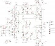
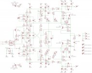
This update enables TSSA BIGBT HP to be even more universal:
- serial diode MUR160 plus 22 ohm resistor in power supply rails helps to improve PSRR
- +/-OPT pins enables to connect separate power supply for the front-end (MUR160 and 22 ohm are omitted)
- power supply LED indicators for both front-end and output stage are present
- serial compensating resistor added to NTC (serves to calibrate NTC thermal response)
- serial resistors added to SK75 heatsink's GND connection (serial RC filter)
- 1 uF/63V decoupling capacitors added close to VAS transistors supply rails
- TLP627 input now accepts 12 V remote signal (serial resistor added)
- LT1034 replaced by TL431
- R2-R9 values stated for +/-50 V power supply rails
And that's about it.
In the moded schematic you swap the two 10R resistors connected to IR led to 100R right?
Marc
In the moded schematic you swap the two 10R resistors connected to IR led to 100R right?
Marc
Temporarily, now are back to 10 ohm.
- TLP627 input now accepts 12 V remote signal (serial resistor added)
That' mean that i can drive TLP627 by my speaker protection board. this use 12V relay mounted on satellite pcb board? I just have to keep sensing wire comming from amp board output (speaker out)
Layout related the schematic above. Output BJT are mounted under PCB but not sandwiched by screew between PCB and heatsink
Just came home from the party
Marc PCB looks great, will do check-up tomorrow, regards Andrej. Hi Andrej,
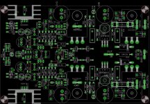
Some more minor cosmetical changes to improve visual symetrie :
-position of tlp627 power supply resistor (to use with 12v)
-position of 10k at signal in.
Some more minor cosmetical changes to improve visual symetrie :
-position of tlp627 power supply resistor (to use with 12v)
-position of 10k at signal in.
Attachments
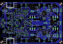
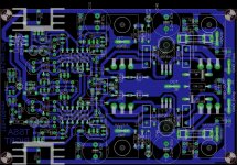
First of all I really have to express my compliments to you for all your work at TSSA BIGBT HP PCB, the board is amazing according to my standards. Look, for only one layer PCB, drawn from medium complex schematic, there's only five wire jumpers, that's is a remarkable achievement. Hats off to you Marc. 
I checked schematic separately and here we go:
- Q7 BF245B, B marking is missing
- C11, C12, C13, C14, C15, C16 are now 100 V marking, if someone will connect optional front-end power supply, that is normally +/- 5-10 V higher than the output power rails. According to given voltages table, front-end rails would be in a response +/- 35-85V. So 100 V capacitor potential marking is on a safe side in all circumstances
- erase GND symbol near C6
- connector J4-1, J4-2 is unnecessary, if there is no need to have remote on/off, than TLP is simply omitted and its pins 3 and 4 are connected with wire jumper
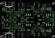
PCB check-up:
- R33, R34 rotate 90° and reposition as now, unisolated part pin too close to PCB edge (elcos can be at the edge - isolated body)
- omit connector J4
- position TLP, R35, LED7 as on pic
- C13, C16 are 100 V, now same diameter as C40, C44
- C12, C15 repositioned
- R23, R24 fliped horizontally
- MUR460 moved away from MJL-s, reposition them as now
- J9, J8 GND connectors moved to middle GND, as now better prevents GND interference currents
We are a tiny dot away from final PCB. Today I will check connections-tracks according to the sch.
Best regards, Andrej
I checked schematic separately and here we go:
- Q7 BF245B, B marking is missing
- C11, C12, C13, C14, C15, C16 are now 100 V marking, if someone will connect optional front-end power supply, that is normally +/- 5-10 V higher than the output power rails. According to given voltages table, front-end rails would be in a response +/- 35-85V. So 100 V capacitor potential marking is on a safe side in all circumstances
- erase GND symbol near C6
- connector J4-1, J4-2 is unnecessary, if there is no need to have remote on/off, than TLP is simply omitted and its pins 3 and 4 are connected with wire jumper
PCB check-up:
- R33, R34 rotate 90° and reposition as now, unisolated part pin too close to PCB edge (elcos can be at the edge - isolated body)
- omit connector J4
- position TLP, R35, LED7 as on pic
- C13, C16 are 100 V, now same diameter as C40, C44
- C12, C15 repositioned
- R23, R24 fliped horizontally
- MUR460 moved away from MJL-s, reposition them as now
- J9, J8 GND connectors moved to middle GND, as now better prevents GND interference currents
We are a tiny dot away from final PCB. Today I will check connections-tracks according to the sch.
Best regards, Andrej
Attachments
I build the super simple version of post one. It worked right away.
(...)
The sound is a bit lighter then with my power buffer ( see MPP ). By adjusting the gain in the preamp and using a warmer sounding cable i got it going. I have to listen more but the amp is very transparent.
Hi Joachim,
I'm considering this as headphone amp. Can you link the final circuit of your MPP (i found the thread but it's huge)?
For a headphone amp this is a bit overdimensioned so be carefull with the volume.
Yeah, I plan to run lower voltage rails like 12-15V. Have to simulate distortion first.
- Home
- Amplifiers
- Solid State
- TSSA - The Simplest Symmetrical Amplifier