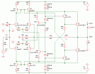
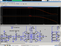
In a previous post i adressed this topology s front end extreme sensitivity
to loading but it seems that it didnt attract much attention...
Anyway , unless the front end i simulated has some nasty flaw ,
the simulations show how much of a problem it can be as soon
as a compensation is implemented.
It s not all to compensate , one must check if the high frequency gain
is effectively used for local NFB or if it is simply dumped by the loading
effect of the compensation network.
To check the thing i simulated the uncompensated OLG and then
loading the FE output with either a resistive or a capacitive load,
the circuit remaining uncompensated so the variation of gain due
to loading can be checked.
Below are the schematic used for sims as well as the graphs
for resistive and capacitive loadings OLGs.
Attachments
Look at ho those transistors behave at lo Vce.
http://www.datasheetcatalog.org/datasheet/HitachiSemiconductor/mXwvryv.pdf
Much inferior to the BC550C or BC337. At 1V Vce the collector impedance ill be abysmal in the current mirror and the Baxandall drivers. Use Cordell's BC550C/560C. You can save those expensive high-voltage japanese transistors for the LTP and Baxandall outputs here they are useful. You NEED lo-Vce transistors for lo-Vce situations like this; high-voltage transistors ork best for high-voltage but ill just saturate in a cascode or current mirror.
The output impedance and loading derive naturally from the input degeneration and Gm, it is a transimpedance stage after all. It is intentional. Any drabacks ill be made up for in other parts of the amplifier. Your LTP degeneration is 100R, Edmund uses 10R IIRC, hich ould make a difference.
See if these changes make an improvement. Actually I don't kno, but I've pointed out some things and am curious about the results.
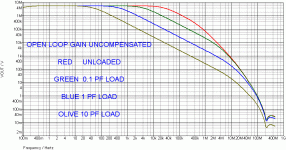
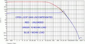
Using 2SC1845/2SA992 ,wich are better than the BCXXX , slightly
improve the thing but still a 10pF load has dreadfull effect on the
high frequency gain while resistive loading allow 100dB OLG
with 1 Mohm load , the gain decreasing as about a linear function
of the resistive load reduction for values lower than about 10 Mohm.
improve the thing but still a 10pF load has dreadfull effect on the
high frequency gain while resistive loading allow 100dB OLG
with 1 Mohm load , the gain decreasing as about a linear function
of the resistive load reduction for values lower than about 10 Mohm.
Did you look at the Vcesat graphs or did you just assume the C1845/A992 are superior because of other specs? I tried them in real life eith my Kmulitpliers. The BC337-25 is best, the BC550C second-best. I don't kno about other gain groups. Again, lo-Vce transistors are best for lo-Vce situations. The 2N5551/5401 are commonly used for current mirrors, but certainly not optimal for that purpose.
They have lower VBE than the BC550 , the BC337 being a medium power
part not used in small signal but rather in low power amplifiers paired
with its complementary BC327 , while all these transistors have low
VCE max not compatible with a front end that has about 100V
supply voltage.
For the sims i reduced the degeneration to 10r , wich seems
to me quite low considering the currents flowing through
the differentials , at about 5.5mA total current.
Did you notice the base current values.?..
part not used in small signal but rather in low power amplifiers paired
with its complementary BC327 , while all these transistors have low
VCE max not compatible with a front end that has about 100V
supply voltage.
For the sims i reduced the degeneration to 10r , wich seems
to me quite low considering the currents flowing through
the differentials , at about 5.5mA total current.
Look at ho those transistors behave at lo Vce.
http://www.datasheetcatalog.org/datasheet/HitachiSemiconductor/mXwvryv.pdf
.
Did you notice the base current values.?..
Last edited:
If you recall I said to save the high-Vce parts for the LTP and Baxandall outputs. So Vcemax as never an issue. I meant to use lo-Vce transistors for the current mirrors and Baxandall drivers here Vce never goes above 1V.
I am talking about mirror output impedance, not mirror imbalance. The C1845 datasheet at 6uA Ib shos a slope of about .5V/1mA hich is the definition of a collector impedance of 500R belo 1V Vce. This is equivalent to 500R shunting your current mirror output. This is because of quasi-saturation. You ill notice that the BC560C and BC337 datasheets sho virtually no quasi-saturation. These transistors have much higher collector impedance at lo Vce. The difference for my Kmultipliers is beteen 48db and 66db of input rejection, or a factor of 8. From a PSRR of 250 to 2k.
Since in this design the current mirrors have a lo-impedance load (Baxandall emitters), raising the 500R mirror impedance may not do much. It may be more critical for the Baxandall drivers hich have just .6V Vce. In a traditional LTP+CM design it can matter a lot because the input of the VAS is a high impedance load. In this position the aforementioned transistors can be a significant improvement over the C1845 or 2N5551.
Hoever most BJT models do not model quasi-saturation. You ill need to check if your models do, otherise they ill not sho you these things.
As a transimpedance stage this circuit has a defined constant transimpedance. The 10R degeneration makes this transimpedance even more constant. They reduce transconductance to about a third. Beyond that I have no explanation offhand for the values.
 .
.I am still interested. Just been busy with the speakers it is intended to power. Now have the compression drivers for the surrounds (JBL 2432's) and the centre channel (JBL 2453) should arrive pretty soon. Now to clear out the workshop to have the space to build it all.
Best wishes
David
Best wishes
David
In a previous post i adressed this topology s front end extreme sensitivity
to loading but it seems that it didnt attract much attention...
Anyway , unless the front end i simulated has some nasty flaw ,
the simulations show how much of a problem it can be as soon
as a compensation is implemented.
It s not all to compensate , one must check if the high frequency gain
is effectively used for local NFB or if it is simply dumped by the loading
effect of the compensation network.
To check the thing i simulated the uncompensated OLG and then
loading the FE output with either a resistive or a capacitive load,
the circuit remaining uncompensated so the variation of gain due
to loading can be checked.
Below are the schematic used for sims as well as the graphs
for resistive and capacitive loadings OLGs.
Why don't you just buffer it and be done with it?
Why don't you just buffer it and be done with it?
See the curves above , the buffer should have less than 1pF and more
than 50 Mohm input capacitance and resistive input impedance respectively ,
so micro meter node fets are required as it s not feasible with discrete components.
For the same reason, an eventual miller compensation must be buffered from
VAS output to its input , using a fet as well.
Last edited:
Thanks Ed. Now it makes sense!
I was wondering about the input filter. This amp must be intended to have a low-impedance source. Audio impedances at the feedback and input nodes are roughly equal, which makes sense. C2 is what I don't understand (your schematic). It is not large enough to bootstrap the input capacitance, which is still somewhere near 2-3nF. I understand the purpose of this arrangement is to achieve a 2nd-order BW limiter, but what does C2 do?
I was wondering about the input filter. This amp must be intended to have a low-impedance source. Audio impedances at the feedback and input nodes are roughly equal, which makes sense. C2 is what I don't understand (your schematic). It is not large enough to bootstrap the input capacitance, which is still somewhere near 2-3nF. I understand the purpose of this arrangement is to achieve a 2nd-order BW limiter, but what does C2 do?
I think phase linearity should be the measure of "cleanliness" of AC/step response. AC response can be flat but have an anomalous step response because of phase nonlinearity. Group delay can be plotted in LTSpice using the Tg() function. The value of 22pF for C2 hardly affects response. Here are my simulated curves with and without C2 (C6 in my schematic).
Attachments
- Status
- This old topic is closed. If you want to reopen this topic, contact a moderator using the "Report Post" button.
- Home
- Amplifiers
- Solid State
- Has anyone seen this front-end before?