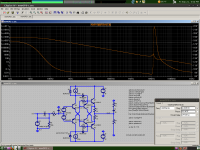
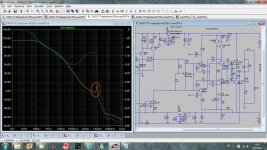
Dadod, you did not exclude the 100k resistor from your input impedance measurement, so the graph did not tell us anything.
This arrangement is extremely unstable. It as oscillating into saturation, hich is hy it did not ork. I got it stable by shaping the source impedance. It ill need some compensation netorks to eliminate the resonance and positive feedback. I haven't tried base stoppers.
Graph shos input impedance.
This arrangement is extremely unstable. It as oscillating into saturation, hich is hy it did not ork. I got it stable by shaping the source impedance. It ill need some compensation netorks to eliminate the resonance and positive feedback. I haven't tried base stoppers.
Graph shos input impedance.
Attachments
The ALT key thing doesn't ork.
Try turning on your num lock key
Hold the ALT down the whole time you are striking the num on the keyboard let the ALT key go AFTER you hit the 9
Still doesn't ork. I'm on Linux, maybe that has something to do ith it.
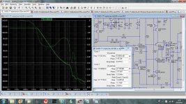
Dadod, you didn't exclude the 100k input resistor in your input impedance graph, so it didn't tell us anything.
This circuit is extremely unstable. Because of this it ould oscillate into saturation and ould appear to not orking. I stopped the oscillation by shaping the source impedance, but the circuit ill need some compensation netorks to eliminate the resonance and positive feedback. One concern ith this circuit is that the drivers have very lo Vce - I don't kno hether it ill ork okay in real life since the models don't have quasi-saturation.
The graph shos input impedance.
Attachments

Dadod, you did not exclude the 100k resistor from your input impedance measurement, so the graph did not tell us anything.
Oh, I am sorry, I totall forgot that it is there.
Still doesn't ork Andre.
I ould not go above 2.2R base stoppers for the outputs, that is simply my preference, but I did find this helped oscillation somehat.
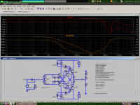
There is still something strange ith your input impedance chart. Check that the Ie (not emitter resistors!) of your outputs is 100mA.
I ould not go above 2.2R base stoppers for the outputs, that is simply my preference, but I did find this helped oscillation somehat.
There is still something strange ith your input impedance chart. Check that the Ie (not emitter resistors!) of your outputs is 100mA.
Still doesn't ork Andre.
I ould not go above 2.2R base stoppers for the outputs, that is simply my preference, but I did find this helped oscillation somehat.
There is still something strange ith your input impedance chart. Check that the Ie (not emitter resistors!) of your outputs is 100mA.
I used 10 ohm base stoppers for predrivers not for the output.
It is 100mA for the output transistors not emitter resistors. I have put this OPS together with my input stage in an amp (simulation) and it does not oscillate but behaves very strange. I switched back to my previous OPS and it is OK with it, no oscillation and it works quite OK.
dado
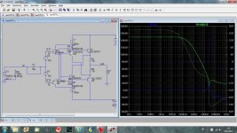
Your output frequency response still indicates that your circuit is oscillating (upturned phase). In a real amp it may ork because the output stage has a high source impedance, but it ill still have the resonance and positive feedback problems hich ill limit it's stability.
This is another example of one of those circuits people tend to dismiss as impossible because they don't kno of any ay to stabilize them... An RC snubber in just the right place can do amazing things. Try this Dadod.
Also notice I rearranged the circuit a bit. It provides the same benefits, but this time the RF current loops are smaller and less convoluted. I like this arrangement better.
Attachments
Your output frequency response still indicates that your circuit is oscillating (upturned phase). In a real amp it may ork because the output stage has a high source impedance, but it ill still have the resonance and positive feedback problems hich ill limit it's stability.
This is another example of one of those circuits people tend to dismiss as impossible because they don't kno of any ay to stabilize them... An RC snubber in just the right place can do amazing things. Try this Dadod.
Also notice I rearranged the circuit a bit. It provides the same benefits, but this time the RF current loops are smaller and less convoluted. I like this arrangement better.
I've had to increas output transistors base stoppers higher then your values to get stable simulation. Attached is the zip LTspice file with two different OPS, my first suggestion and your last one.
I am not satisfied with nether of them, but if you can make anything of it, please show it.
dado
Attachments
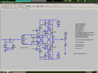
Your first circuit ithout the BC5xx collectors bootstrapped may need different compensation than the RC.
If you consider each difference beteen this output stage and a traditional EF, you'll see that it's essentially optimized for speed. As for distortion, there are a lot of intervening factors, such as the quality of the 100mA CCS's, and quasi-saturation of the drivers. In the end the circuit is biased at the margins. So I agree that this arrangement leaves us anting more.
Again, the MJE1503x are overkill for the CCS's, MJE253/243 are perfectly safe here and probably ill perform better. But the BC5xx are not prepared for 80V Vce at max volume. You could try a simple capacitor bootstrap (attached). It is pretty much a free mod, since they only have 2mA Ic. Interestingly the RC's are still needed here.
Furthermore, putting the CCS's after the diode in the C-multiplier may be a bad idea. For one thing, you limit voltage range again and it is the voltage range of the CCS hich limits this output stage. Secondly, look at the diode as a filter device. At 10mA it is about 2.5R. By moving the CCS here you increase it's bias to 100mA hich decreases it's resistance to .25R, reducing its filtering ability by a decade. No it is basically doing nothing, and actually reduces the benefit that the proceeding circuitry gets. I think it is better to hang the CCS off the main rails.
Also, look at the Ib of Q23 and Q25. If the Hfe of these transistors is say 100, then Ib ill be 1mA. R44 conducts about 1.6mA. The 1mA ill be gobbled up by Q23/25 and ill leave only .6mA for Q24/26. It could be orse; if R44 as 100k there ould be a measely 100uA left for Q24/26 and this ould cause them to saturate hile driving the bases of Q23/25 and cause glitches and high order distortion. Furthermore, consider the logarithmic behavior of the Vbe of Q24/26. ith 1mA Ic, they ill have a transresistance of about 33R. This is seen in parallel ith R38 and R41. 33/5.6=5.9. So any current variations through R44 ill be magnified in the CCS output current by about 6 times! So I ould decrease R44 to 27k or so, though it may dissipate more.
Attachments
My most interesting prototype yet is on the bench. It has 3 20-turn trimmers and 2 1-turn trimmers. It uses a clever self-feedback output stage that eliminates current AND voltage distortion from the output stage, loosening requirements for the frontend. The output stage itself performs ell enough to be used ithout a frontend (belo .01% THD at 5A into 6R ith one pair of outputs) depending on your personal standards of course. The output stage has just 6 transistors. The frontend is a buffered single-ended non-LTP thingy hich presents a sort of fussy challenge. The VAS is almost, but not entirely, unremarkable. I have to mess ith time constants to get the hole circuit to start up properly.
It is also my most compact point-to-point iring job. All 15 transistors, 30 resistors, and 18 capacitors fit very tightly in 4 cubic inches, ith most of the mass in the middle. I am considering submitting it to a local art (sculpture?) sho to see just ho far this circuit can take me. I had to sandich some aluminum foil in some masking tape and edge it in the thing to shield more sensitive traces from the output and VAS. I should probably be a bit more careful of layout.
I just anted to update for anyone ho might have an interest in my affairs. I no yield to the topic flo...
Your first circuit ithout the BC5xx collectors bootstrapped may need different compensation than the RC.
If you consider each difference beteen this output stage and a traditional EF, you'll see that it's essentially optimized for speed. As for distortion, there are a lot of intervening factors, such as the quality of the 100mA CCS's, and quasi-saturation of the drivers. In the end the circuit is biased at the margins. So I agree that this arrangement leaves us anting more.
Again, the MJE1503x are overkill for the CCS's, MJE253/243 are perfectly safe here and probably ill perform better. But the BC5xx are not prepared for 80V Vce at max volume. You could try a simple capacitor bootstrap (attached). It is pretty much a free mod, since they only have 2mA Ic. Interestingly the RC's are still needed here.
Furthermore, putting the CCS's after the diode in the C-multiplier may be a bad idea. For one thing, you limit voltage range again and it is the voltage range of the CCS hich limits this output stage. Secondly, look at the diode as a filter device. At 10mA it is about 2.5R. By moving the CCS here you increase it's bias to 100mA hich decreases it's resistance to .25R, reducing its filtering ability by a decade. No it is basically doing nothing, and actually reduces the benefit that the proceeding circuitry gets. I think it is better to hang the CCS off the main rails.
Also, look at the Ib of Q23 and Q25. If the Hfe of these transistors is say 100, then Ib ill be 1mA. R44 conducts about 1.6mA. The 1mA ill be gobbled up by Q23/25 and ill leave only .6mA for Q24/26. It could be orse; if R44 as 100k there ould be a measely 100uA left for Q24/26 and this ould cause them to saturate hile driving the bases of Q23/25 and cause glitches and high order distortion. Furthermore, consider the logarithmic behavior of the Vbe of Q24/26. ith 1mA Ic, they ill have a transresistance of about 33R. This is seen in parallel ith R38 and R41. 33/5.6=5.9. So any current variations through R44 ill be magnified in the CCS output current by about 6 times! So I ould decrease R44 to 27k or so, though it may dissipate more.
I wanted to simulate this OPS behavior i GNFB. I just used my old amp's input stage and the diodes in the power lines are left over from it, but it does not influance main goal, to show how stable is the OPS in GNFB amp.
You are correct about R44, it was way to high, now it is 10k(dissipation isnot a problem) and CCS works better, but the main problem is high peak at 9MHz. It could be tamed the with the RC at the output transistors bases.
Can you show the schematic of that yours amp prototype, or OPS only?
dado
Attachments
Changing Q23 and Q25 to MJE253/243 ill partly help the 10MHz spike. You may also try collector resistors on these transistors as a clever ay of inserting damping. You can see it this ay: the VAS output impedance has more than 90 degree phase shift. The OPS input impedance also has more than 90 degrees phase shift. This is because in both cases, capacitors are bootstrapped. Much of the amp's stability characteristics are determined by this junction and if the combination of the source and input phase gets too high, you get a local oscillator or at least a troublesome resonator. This is a big Caveat Emptor hen it comes to using bootstrapping and cascoding to eliminate parasitic capacitances; you only eliminate them at audio frequencies - at RF they become sources of phase dismay.
Other than that I ended up increasing the RC values to 68n/.33R to try and get rid of the 10MHz spike. This asn't very satisfying.
I ould like to share my OPS but I'm still trying to ork out the thermal behavior. I have shared it ith one person ho as going to build it but hasn't gotten around to it yet. It is thermally stable at 20V but hen the supply increases to 30 or 40 volts it starts doing the 2-steps-forard, 1-step back-thing and it makes me anxious. There must be such a thing as thermal oscillation.
Changing Q23 and Q25 to MJE253/243 ill partly help the 10MHz spike. You may also try collector resistors on these transistors as a clever ay of inserting damping. You can see it this ay: the VAS output impedance has more than 90 degree phase shift. The OPS input impedance also has more than 90 degrees phase shift. This is because in both cases, capacitors are bootstrapped. Much of the amp's stability characteristics are determined by this junction and if the combination of the source and input phase gets too high, you get a local oscillator or at least a troublesome resonator. This is a big Caveat Emptor hen it comes to using bootstrapping and cascoding to eliminate parasitic capacitances; you only eliminate them at audio frequencies - at RF they become sources of phase dismay.
Other than that I ended up increasing the RC values to 68n/.33R to try and get rid of the 10MHz spike. This asn't very satisfying.
I ould like to share my OPS but I'm still trying to ork out the thermal behavior. I have shared it ith one person ho as going to build it but hasn't gotten around to it yet. It is thermally stable at 20V but hen the supply increases to 30 or 40 volts it starts doing the 2-steps-forard, 1-step back-thing and it makes me anxious. There must be such a thing as thermal oscillation.
Here is my last incarnation of the amp with new OPS. THD20k is 0.81ppm at 70 W on 8 ohm.
I am not completely satisfied with the Gain Margin and how the phase twists around 15 MHz.
I simulated the CCS with MJE253/243 instead MJE15032/15033 with no differences at all, so I keep the more powerful pair here as the power dissipation go up to 9 W on the CCS. I tried MOSFET CCS with DN2540 with similar result.
Big question here is how to go for more output pairs??
I did not scratch thermal stability yet.
dado
Attachments
100mA max base drive for the outputs, means 10A max output for an Hfe of about 100. So an extra pair can still make use of the measely max 100mA drive since the outputs lose Hfe after 6A. But after 3 pairs or so you ill run out of drive at max volume; then you ill need to increase CCS current or add an extra pair of drivers.
Bypassing electrolytic caps.
Glen has updated his website with measurement on larger (electrolytic) caps.
See also: Bypassing large electro's with smaller caps - Page 1 for additional info.
Thx Glen!
Cheers,
E.
Glen has updated his website with measurement on larger (electrolytic) caps.
See also: Bypassing large electro's with smaller caps - Page 1 for additional info.
Thx Glen!
Cheers,
E.
- Status
- This old topic is closed. If you want to reopen this topic, contact a moderator using the "Report Post" button.
- Home
- Amplifiers
- Solid State
- Has anyone seen this front-end before?