Edmond, interesting comments about the bipolar vs JFET input! Very difficult now to get matched JFETS, so I guess the fact that they are unobtainium just drives up their street cred . . . but I doubt there is anything magical about them.
That said, for single ended designs they are ok, but a degenerated bip is just as good if not better other than the noise from the degen resistors, but thi sis not an issue on a power amplifer IMO.
Anyway, I really enjoy reading your stuff - very nice - please keep it coming.
That said, for single ended designs they are ok, but a degenerated bip is just as good if not better other than the noise from the degen resistors, but thi sis not an issue on a power amplifer IMO.
Anyway, I really enjoy reading your stuff - very nice - please keep it coming.
Hi Andrew,
Thank you for your encouraging words.
>please keep it coming.
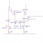
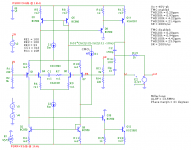
I did just that. See fig.17: SuperTIS + Bod Cordell's HEC output stage.
Cheers,
E.
PS >but a degenerated bip is just as good if not better other than the noise from the degen resistors,
They are just 10 Ohms. So, not much to worry about the added noise.
Thank you for your encouraging words.
>please keep it coming.
I did just that. See fig.17: SuperTIS + Bod Cordell's HEC output stage.
Cheers,
E.
PS >but a degenerated bip is just as good if not better other than the noise from the degen resistors,
They are just 10 Ohms. So, not much to worry about the added noise.
Last edited:
More on RFI
The previous RFI sims made me suspicious. Therefore I've repeated the sims with a smaller HF signal: 100mV instead of 1V.
Now the differences between AM detection levels and compression distortion are far less extreme.
See also my website.
Cheers,
E.
The previous RFI sims made me suspicious. Therefore I've repeated the sims with a smaller HF signal: 100mV instead of 1V.
Code:
Front-end:               SuperTIS-BJT   SuperTIS-JFET   HEC-BJT    HEC-JFET
Demodulated AM signal:      5.4uV          1.26mV       0.35mV      0.82mV
THD20k without HF carrier:  0.028ppm       0.071ppm     0.19ppm     0.76ppm*
THD20k with HF carrier:     0.030ppm       0.072ppm     0.24ppm     26.3ppm
THD20k increase:            0.002ppm       0.001ppm     0.05ppm     25.5ppm
Now the differences between AM detection levels and compression distortion are far less extreme.
See also my website.
Cheers,
E.
Last edited:
high Z & phase margin
Hi JCX,
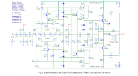
Your absolutely right. As a matter of fact, it needs a very high input Z. Driving for example Bob's HEC-OPS directly (i.e using Bob's Q20 & Q21 as pre-driver ), yields less favorable results. But... using a separate pre-driver, configured as diamond buffer with bootstrapped collectors, works nice: THD20k = 3.1ppm (without TMC). See fig.17.
Indeed, that's another point of concern. The amp of fig.12 for example, has a phase margin of only 50 degrees (seen at the output). Seen at the input it's much better: 94 degrees, but it is the lowest value that counts. So I definitely have to improve this figure, at least to 60 degrees.
Cheers,
E.
[..]
- I expect best performance would had with error corrected/local feedback output stage giving high input Z, gain close to 1
Hi JCX,
Your absolutely right. As a matter of fact, it needs a very high input Z. Driving for example Bob's HEC-OPS directly (i.e using Bob's Q20 & Q21 as pre-driver ), yields less favorable results. But... using a separate pre-driver, configured as diamond buffer with bootstrapped collectors, works nice: THD20k = 3.1ppm (without TMC). See fig.17.
will be interesting to see stability with all of the nested feedback around the output Q.
[..]
Indeed, that's another point of concern. The amp of fig.12 for example, has a phase margin of only 50 degrees (seen at the output). Seen at the input it's much better: 94 degrees, but it is the lowest value that counts. So I definitely have to improve this figure, at least to 60 degrees.
Cheers,
E.
Last edited:
Hi JCX,
Your absolutely right. As a matter of fact, it needs a very high input Z.
Cheers,
E.
About how high? Presumably it's asymptotic, so plot of THD20 versus load Z would be nice, but otherwise just an approximate number for a reasonable load would help .
Best Wishes
David
BTW re. your earlier post - Scotland is british.
(Britain is Wales, Scotland and that bit in the middle)
Indeed, it's problematic to do it with a conventional circuit, as too many stages are enclosed by the Miller loop. It will result in too much gain and too much phase shift. Perhaps one can tame such an arrangement by means of an additional massive lead-lag compensation, but most likely that is counter productive.
It's not obvious to me why it would be much worse with the conventional circuit. The IPS is identical in both. From the pre-driver onwards it is also (for comparison) identical. The difference is a Baxandall pair compared to, say, the usual VAS pair with the emitter follower before the CE.
If simulation results are very different I'd appreciate an explanation of why.
And if there is too much gain then perhaps it could be used beneficially via nested Miller compensation rather than create problems with massive shunt compensation. That's my main query. The differences in alternative shunt compensation placements is educational but for a fall-back option.
Best wishes
David.
I have a new collection of minor typos if you want them. Would you prefer a PM?
Zi
Hi David,
Zi = 770kOhms @ 20kHz was apparently too low, because THD20k = 21ppm
With a diamond pre-driver Zi = 96MOhms @ 20kHz and THD20k = 3.1ppm, which is okay.
That is, after Scotland became part of the Kingdom of Great Britain in 1706, right?
But my great^n granny lived in 16th century.
Cheers,
E.
About how high? Presumably it's asymptotic, so plot of THD20 versus load Z would be nice, but otherwise just an approximate number for a reasonable load would help .
Best Wishes
David
Hi David,
Zi = 770kOhms @ 20kHz was apparently too low, because THD20k = 21ppm
With a diamond pre-driver Zi = 96MOhms @ 20kHz and THD20k = 3.1ppm, which is okay.
BTW re. your earlier post - Scotland is british.
(Britain is Wales, Scotland and that bit in the middle)
That is, after Scotland became part of the Kingdom of Great Britain in 1706, right?
But my great^n granny lived in 16th century.
Cheers,
E.
Great Britain, UK, British Isles, etc. all have their own quite precise but different definitions.
The green & blue Euler diagram depicts it well. It's about half way down.
British Isles - Wikipedia, the free encyclopedia
The green & blue Euler diagram depicts it well. It's about half way down.
British Isles - Wikipedia, the free encyclopedia
It's not obvious to me why it would be much worse with the conventional circuit. The IPS is identical in both. From the pre-driver onwards it is also (for comparison) identical. The difference is a Baxandall pair compared to, say, the usual VAS pair with the emitter follower before the CE.
If simulation results are very different I'd appreciate an explanation of why.
And if there is too much gain then perhaps it could be used beneficially via nested Miller compensation rather than create problems with massive shunt compensation. That's my main query. The differences in alternative shunt compensation placements is educational but for a fall-back option.
Best wishes
David.
Hi David,
I'm afraid we are at cross purposes, aren't we? I thought you meant by 'a conventional circuit' something like the 'blameless' IPS and VAS, including a 'beta enhancement' tranny. It's this circuit that is incompatible with input inclusive compensation (at least, without additional measures to tame it), because the compensation encloses too many stages with gain.
>The difference is a Baxandall pair compared to, say, the usual VAS pair with the emitter follower before the CE.
The current gain of the Baxandall pair is just 1x, while the current gain of usual VAS pair with EF is about 10000x. That's a huge difference.
Anyhow, please correct me if I misunderstand you.
I have a new collection of minor typos if you want them. Would you prefer a PM?
Yes, please!
Cheers,
E.
Any thoughts abt adding an inner current mirror to the long tail pair?
Hi Ronny,
Since seeing only a (small) part of the circuit, I don't know what to think about it. Could you provide a complete circuit, please?
Also, I like to hear what the purpose is of the inner current mirror.
Cheers,
E.
To get such low distortion or very close to it it’s possible with much simpler schematic if nice and eyes catching symmetric design is not a paramount.
As there is no perfect amplifier, D Self called his design “blameless” and I like his approach very much. He was not using a Triple Output Stage and Two-Pole Compensation. If we include those in the circuit a distortion became very low and with some better input stage we are there.
I like Edmond circuits a lot, specially his Auto-Bias circuit(I hope I will find a time to implement that in one of my next amps) but the circuit became so complicate that layout PCB design is not DIY any more. It will be very nice to have Edmond’s designs put in practice and hear the listening impressions.
Here I have two much simpler amps, one with TMC(bridged TMC actually, and could we call it BTMC) and one with bridged TPC or BTPC with distortion very close to the Edmond’s TIS + Auto-Vias II amp.
dado
Attachments
Hi Damir,
Indeed, you circuit is unmistakably simpler, in particular the output stage.
(though the input stage is of comparable complexity, 15 versus 18 trannies).
Yet THD levels are on the same level. Several factors account for this:
1. An BJT OPS produces less distortion than a MOSFET OPS.
2. An auto bias circuit produces more distortion, due to modulation of the bias voltage.
3. The transition frequency of you TMC circuit is a bit higher.
I believe these are the main factors that should explain why your simpler amp performs so well.
>It will be very nice to have Edmond’s designs put in practice and hear the listening impressions.
I don't harbor any illusion that my amp will sound special. Maybe it will sound uninterestingly or even dull,
because a good amp (read: neutral amp) amp has no particular sound at all.
Cheers,
E.
Hi Ronny,
Since seeing only a (small) part of the circuit, I don't know what to think about it. Could you provide a complete circuit, please?
Also, I like to hear what the purpose is of the inner current mirror.
Cheers,
E.
Change of input gm, and in these inviromental frendly times reduse power consumtion just a fraction
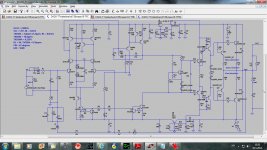
Attachments
I'm afraid we are at cross purposes, aren't we? I thought you meant by 'a conventional circuit' something like the 'blameless' IPS and VAS, including a 'beta enhancement' tranny. It's this circuit that is incompatible with input inclusive compensation (at least, without additional measures to tame it), because the compensation encloses too many stages with gain.
>The difference is a Baxandall pair compared to, say, the usual VAS pair with the emitter follower before the CE.
The current gain of the Baxandall pair is just 1x, while the current gain of usual VAS pair with EF is about 10000x. That's a huge difference.
Anyhow, please correct me if I misunderstand you.
Yes, perhaps cross purposes so let me clarify.
A complementary IPS I assume as obvious
so no Self "blameless".I mean to compare the barebones (current mirrored, complementary symmetrical) SuperTIS with an equivalent barebones, current mirrored, complementary symmetrical VAS.
So they would be similar except that the transistors that form Baxandall pairs in the SuperTIS would be reconnected to form beta enhanced VASes, with appropriate adjustments to current sources.
I understand this barebones Comp.Sym VAS is not practical due to quiescent current stability and I appreciate the neat way that the SuperTIS solves the problem. But it should simulate OK.
Now if we apply Input Inclusive compensation to both of them then it will enclose identical number and types of transistors. The conventional VAS has more current gain, as you say. Does it matter?, the feedback point at the input transistor is high impedance and the Baxandall Q10 and Q11 have voltage gain yes? So I want to understand this a bit better.
Best wishes
David.
Conventional circuit with IIC
Hi David,
Now I completely understand what you mean, see below. After some modifications I got this circuit more or less stable. The emitter degen. resistors had to be increased from 10 to 100 Ohms and C1 from 1 to 3.3nF. Nevertheless, the phase margin of the Miller loop is a meagre 41 degrees and difficult to improve. Compared to the superTIS, the distortion is three to four times higher and the slew rate half as high. Apart from the need of some form of a CMCL, I would conclude that this circuit is suboptimal.
Cheers,
E.
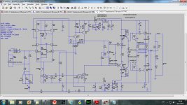
Attachments
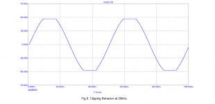
20 Khz clipping response
Hello Edmond,
On your website you post the following graph, I was wondering which actual circuit schematic you used to generate this was it fig 6.
The reason I ask is my clipped waveform sims are not as clean as yours.
Regards
Arthur
Hello Edmond,
On your website you post the following graph, I was wondering which actual circuit schematic you used to generate this was it fig 6.
The reason I ask is my clipped waveform sims are not as clean as yours.
Regards
Arthur
Attachments
- Status
- This old topic is closed. If you want to reopen this topic, contact a moderator using the "Report Post" button.
- Home
- Amplifiers
- Solid State
- Has anyone seen this front-end before?