Hi Harry,
I often like to make sure there is an electrolytic somewhere on a line that is bypassed with an electrolytic to prevent resonance, since the ESR of the electrolytic helps damp any resonance, especially among ceramics separated by trace inductance. I've never seen a resonance problem between an electrolytic and a ceramic.
Cheers,
Bob
You meant an electrolytic on a line that is bypassed with a ceramic, I suppose?
dado
You meant an electrolytic on a line that is bypassed with a ceramic, I suppose?
dado
Correct - sorry for the mistake.
Cheers,
Bob
At rated voltage - you sure about that? The curves I've seen IIRC show capacitance dropping off very significantly when applied voltage is much less than rated.
Yes, attached are my measurements so far; brands are anonymised to avoid anyone getting upset!
You said to put in parallel with ceramics, series RC. What value for C and what kind? I use 0.1u for ceramics.
Dado
This is something that's fairly straightforward to simulate. Use a full L-C-R model for all your caps and then simulate the impedance vs. frequency. Make sure there aren't any unpleasant peaks. X7R ceramics will suffice for the Cs in the RC networks, if they turn out to be required.
According this document X7R should not lose so much: http://www.wolfsonmicro.com/document...en/WAN0176.pdf
Sadly that document is wrong. Murata do publish the voltage coefficient of some of their caps (e.g. here); this can be used to verify that my measurements are accurate (or at least, agree with Murata's!).
since the ESR of the electrolytic helps damp any resonance, especially among ceramics separated by trace inductance. I've never seen a resonance problem between an electrolytic and a ceramic
You can't make a blanket statement that the ESR of the electrolytic will prevent resonance. It will depend on the specific electrolytic: how far apart are its pins (this dominates the series inductance) and what is its ESR? Low ESR and high inductance is the worst combination. Again, this can be modelled. In theory, if you have a ground plane you can even predict an L-C-R model of the power traces, using a lumped model up to approx 80 mm in length for frequencies up to 200 MHz. I'm working on verifying the theory next week with some impedance measurements of a two-layer board.
Attachments
Correct - sorry for the mistake.
Cheers,
Bob
Hello Bob,
Do you bypass an electrolytic directly on the back side with a ceramic, or put a ceramic close were + - power lines enter the PCB?
Thanks Damir
You can't make a blanket statement that the ESR of the electrolytic will prevent resonance. It will depend on the specific electrolytic: how far apart are its pins (this dominates the series inductance) and what is its ESR? Low ESR and high inductance is the worst combination. Again, this can be modelled. In theory, if you have a ground plane you can even predict an L-C-R model of the power traces, using a lumped model up to approx 80 mm in length for frequencies up to 200 MHz. I'm working on verifying the theory next week with some impedance measurements of a two-layer board.
Then let me be more specific. I have never seen a resonance problem between a 0.1uF ceramic and an aluminum electrolytic whose capacitance was between 10uF and 100uF and where the leads between the two capacitors were less than 1/2 inch each.
What values of ESR and inductance are you assuming for electrolytics that you work with?
Cheers,
Bob
Hello Bob,
Do you bypass an electrolytic directly on the back side with a ceramic, or put a ceramic close were + - power lines enter the PCB?
Thanks Damir
I always put all components on the component side. Where there is an electrolytic bypassed with a ceramic, the ceramic is right next to the radial electrolytic. I always put an electrolyic bypassed with a ceramic where + and - lines enter the PCB. Unless needed for reasons of current or voltage drop, I do not attempt to make the wires carrying the rail voltages to the board of heavy guage (e.g., for powering of small-signal circuits).
Cheers,
Bob
Basics of Ceramic Chip Capacitors
You are right. Capacitance declines with applied voltage. What I am surprised is that at the rated voltage the capacitance in your graphs is a fraction of its specified value.
You are right. Capacitance declines with applied voltage. What I am surprised is that at the rated voltage the capacitance in your graphs is a fraction of its specified value.
You are right. Capacitance declines with applied voltage. What I am surprised is that at the rated voltage the capacitance in your graphs is a fraction of its specified value.
Yes, the manufacturers like to keep this quiet, don't they*? Y5V are even worse! Let's not forget that this is just the effect of DC bias and you can lose up to a further 15% capacitance (for X7R, 82% (!) for Y5V) if temperature is varied.
*If you read the small print of the data sheet, they will note that the "specified capacitance" is for zero DC bias, not the rated DC voltage; graphs (or any info at all) detailing voltage coefficient is not usually provided.
Last edited:
Hello Bob,
Do you bypass an electrolytic directly on the back side with a ceramic, or put a ceramic close were + - power lines enter the PCB?
Thanks Damir
To determine where you should place decoupling caps, trace out the current pathway and place the caps to minimise the enclosed loop area. Placing the ceramics right next to the electrolytics is pointless if the electrolytics are far away from the point at which you're trying to minimise supply impedance. For a linear power amp, pretty much the only current that will flow in ceramic bypass capacitors is the zobel current, assuming the layout is right. If the layout doesn't minimise the loop area of the current path of HF decoupling cap -> active device -> zobel, the HF decoupling cap will do pretty much nothing.
What values of ESR and inductance are you assuming for electrolytics that you work with?
In a class-D stage I've designed but not built yet I will be using 330 uF aluminium electrolytics with 50 mR ESR and approx 10 nH inductance. If paralleled with a 1206-sized 220 nF ceramic, there will be a resonance at approx 3.2 MHz.
That looks a good place for the ceramic decoupling capacitors* but only if you place the emitter traces of the output transistors on top of (or underneath) the collector traces and bring the zobel ground to the ceramics' ground connection.
Harry,
I changed the zobel ground, but how to place the emitter traces of the output transistors on top of (or underneath) the collector traces I am out of ideas. Is that so impotant as emitter currents are low distortion music signals???
Damir
Attachments
![DADO-TT-TMC-7-2-g-1.LAY].jpg](/community/data/attachments/280/280482-f8c70bc316656413bca26610b484efe9.jpg)
Harry,
I changed the zobel ground
We're talking C99 and R99, correct? The ground connection needs to be made at the same point as the ground of the ceramics; currently it is not.
but how to place the emitter traces of the output transistors on top of (or underneath) the collector traces I am out of ideas
That would require a somewhat more fundamental change to your layout. Also for maximum fun, you could make the +ve and -ve pathways perpendicular to one another (try orienting the output devices at 45 degrees, to make an inverted "v" shape: the NPN devices forming one edge of the "v", and the PNP devices the other edge)
is that so impotant as emitter currents are low distortion music signals???
Damir
The emitter traces only carry low-distortion music signals once they have mixed. Before the join, the +ve and -ve pathways are rich in high-order harmonics. Placing collector paths on top of emitter paths minimises inductance and possibility of radiation.
Last edited:
We're talking C99 and R99, correct? The ground connection needs to be made at the same point as the ground of the ceramics; currently it is not.
Sorry, there is additional wiring from the back side. Showed are the wires to the PSU and the loudspeaker too. I think that you suggested this way to connect the loudspeaker.
I prefare to use aluminium L bracket to mount output transistor and that requires the transistors in a line arrengement. In that way I can finish whole amp board and test it outside the box. Additional, it is much easier to service as whole amp board together with output transistors by fixing it to the temporary heat sink. Some thinks that this configuration could provoke the output transistors over heating as a consequence of not so good heat transfer, but I never had any problem with it.
dado
Attachments
![DADO-TT-TMC-7-2-g-2.LAY].jpg](/community/data/attachments/280/280531-6940b5405a468bea5b4f359478a55adb.jpg)
Harry,
...........
but how to place the emitter traces of the output transistors on top of (or underneath) the collector traces I am out of ideas.
...........
Damir
Damir,
Indeed, it's impossible do that, that is, all the the way from begin to end. But you can neutralize the loop area, see my post about the lemniscate trick #876.
Cheers,
E.
I have measured resonance as ell. I had 3 470nF MKT films, beteen rails and ground, and the third beteen the rails. These caps ere separated in trace length by only a fe inches but the resulting resonance alloed my output stage to oscillate. My problem as that the main lytic reservoirs ere several inches of tisted alligator clips aay. I had to add 120uF caps directly to the prototype hich as air-ired. Lo-impedance lytics can oscillate as ell. It is alays best to simply check your rails ith a sept sine generator, and/or model the trace inductances and capacitors in SPICE. A 1uF RC can be used but a lytic ill take up less space, although ho knos ho it's ESR might vary ith time.
I have a problem. My keyboard is missing a button and my mouse doubleclicks itself every time (has been for several months). Maybe I have too much patience ith these things...
I have a problem. My keyboard is missing a button and my mouse doubleclicks itself every time (has been for several months). Maybe I have too much patience ith these things...
Damir,
Indeed, it's impossible do that, that is, all the the way from begin to end. But you can neutralize the loop area, see my post about the lemniscate trick #876.
Cheers,
E.
Thanks Edmond,
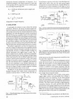
It is not easy to make good layout. I've got Cherry's article, I think you mentioned this one.
Damir
Attachments
look at the PCB layout.
The two traces for speaker output have all their connections away to the right hand side.
I can see no advantage to bringing the speaker output to the left alongside the input traces. Take the speaker out from the middle of the PCB and delete the unnecessary traces.
The 10r signal gnd to power gnd link could be moved to tap in to the right hand side of the hatched area. Then all of the output traces are to that same right hand side.
Does the power input need to be fed from the left?
Or would it be better to feed power into the right hand side? Then bring the low current power traces to the left hand side.
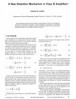
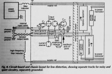
I note that Cherry is using the Chassis as the Main Audio Ground. Is this the best way? Or should there be a separated Main Audio Ground with a tapping to the Chassis to gain the screening effect of the enclosing case?
The two traces for speaker output have all their connections away to the right hand side.
I can see no advantage to bringing the speaker output to the left alongside the input traces. Take the speaker out from the middle of the PCB and delete the unnecessary traces.
The 10r signal gnd to power gnd link could be moved to tap in to the right hand side of the hatched area. Then all of the output traces are to that same right hand side.
Does the power input need to be fed from the left?
Or would it be better to feed power into the right hand side? Then bring the low current power traces to the left hand side.
I note that Cherry is using the Chassis as the Main Audio Ground. Is this the best way? Or should there be a separated Main Audio Ground with a tapping to the Chassis to gain the screening effect of the enclosing case?
Last edited:
look at the PCB layout.
The two traces for speaker output have all their connections away to the right hand side.
I can see no advantage to bringing the speaker output to the left alongside the input traces. Take the speaker out from the middle of the PCB and delete the unnecessary traces.
The 10r signal gnd to power gnd link could be moved to tap in to the right hand side of the hatched area. Then all of the output traces are to that same right hand side.
Does the power input need to be fed from the left?
Or would it be better to feed power into the right hand side? Then bring the low current power traces to the left hand side.
Sorry Andrew I am not sure what PCB layout you are talking about, there is double side one and single side one.
Damir
- Status
- This old topic is closed. If you want to reopen this topic, contact a moderator using the "Report Post" button.
- Home
- Amplifiers
- Solid State
- Has anyone seen this front-end before?