Guys
I changed Q401, Q403, Q405 and pretty much all semiconductors as suggested and also the 139 again.
I've also had to repair the track as I damaged it with all the putting in and ripping out again, looks as if they're not designed for that though.
The amp now runs ok at full line voltage.Voltage measurements seem similar for both side now too. I've set up the centre voltages, but the idling current on the previously blown side does not seem to be adjustable. The pot is ok.
With the solder shorts removed as per instructions one channel (the one that was ok to start) is adjustable but the 'repaired' by me side is not. I cannot see any voltage across the testpoints.
Having said that, the unit has been running at a high volume for over an hour now and seems to be performing ok on both sides.There is no sign of overheating.
Thanks to all that have been kind enough to offer guidance to me. If anyone would like to comment regarding the idle current adjustment I would be interested.
thanks
Paul
As you have now added emitter resistors to the amp, forget the solder shorts that measure over the 1R resistor. Instead, measure the voltage drop over one of the emitter resistors. From that, you can calculate your bias current. Vdrop / Remitter = Ibias. The original instructions suggest 28mA of bias.
It should change when you turn R443. If it doesnt, something is wrong. Q409, with R439, D405, R441, R443, R445 form what is called a VBE Multiplier or "amplified diode".
Basically, it's a constant voltage source. The idea is that it biases the output transistors on slightly to avoid the crossover region - i tend to think of it much like the idle speed of a car engine.
Another crucial part is that the VBE multiplier provides thermal feedback. You will see that the BD139 used is attached to the heatsink with the power transistors. This is so as the outputs warm up, the bias is kept constant. If it was not there, the result would be thermal runaway - as the transistors heat, the bias current would increase, until the output transistors overheat and fail. This is why you need to be sure that the VBE Multiplier stage is working correctly.
I'd recommend a good look at Rod Elliot's various articles: DIY Audio Articles
Great job staying with it and not giving up until you found the answer! Looks like NAD has sucked another person into DIY...
I second jaycee's recommendation to read Rod Elliot. When you're ready for the next step, Bob Cordell's book does a fantastic job of being informative and useful to experienced engineers and simultaneously accessible and understandable to beginners.
I second jaycee's recommendation to read Rod Elliot. When you're ready for the next step, Bob Cordell's book does a fantastic job of being informative and useful to experienced engineers and simultaneously accessible and understandable to beginners.
I've started reading Rod Elliot now, and very interesting it is too, easy to lose hours looking at the monitor! I'll be checking out Bob Cordell as well...so many things ...so little time... ")
Thanks very much everyone.
I'm just eying up a function generator and having a look for a new scope, my scope is 30 years old and rather creaky now. so many to chose from....
Thanks very much everyone.
I'm just eying up a function generator and having a look for a new scope, my scope is 30 years old and rather creaky now. so many to chose from....
Had a lot of these amps ,always seem to blow up every 10 years ,the 2SD669A and the 2SB649A transistors are in stock at electronic component suppliers and distributors, Nikko Electronics for semiconductors, transistors, capacitors all major brands of spare and replacement parts ,search for 2SD669AC ,both 5A fuses blown , 2N3055 S/C ,,2SD669 S/C collector to emitter ,
i replaced the 2SD669A with an exotic part until i get the parts from Nikko ,works fine
anyone know what the bias current is ? i can measure it across the 0.33 R emitter resistors
i replaced the 2SD669A with an exotic part until i get the parts from Nikko ,works fine
anyone know what the bias current is ? i can measure it across the 0.33 R emitter resistors
Hi All!
I know this thread is old, but it was extraordinarily helpful to me while I was repairing my 7220PE. Like the 7225 and the 701, the 7220PE shares the old 3020 power amp section, reference designators and all.
Like p10ness, when I completed my transistor swap, I too was experiencing 0mV offset while trying to set the idle current of the newly restored channel. However, I did figure out the problem.
The new devices I used apparently need just a smidge MORE current to turn on than the original drivers and output stages.
So, I needed to change the "battery" circuit slightly. The original design shows a 100-ohm resistor in the R441 and R442 locations. While this works great for the original components, my newer components did NOT turn on at idle with this vale.
So, I changed R442 of my previously blown channel to a 68-ohm resistor. This allows more current through the "battery" circuit and the newer devices turn on properly at idle. With this change, I was able to properly set the idle current.
FWIW, I used MJ15022/23 output transistors and KSA1220A/KSC2690A drivers. I also replaced all the other transistors in the circuit with the lead-free "G" versions. Finally, I also replaced all the electrolytic caps in the power amp and preamp sections with Elna Similic 2 or Nichicon FG caps.
For now, I've got one channel left as original and one channel with all the above changes. I'm going to let things settle in for a few days on the new caps and transistors, then I'm going to do an "old-school" versus "new-school" comparison. Basically, I want to find out if changing the FETs and caps to newer, modern audio devices really makes the big difference.
I'll report back when I have more details, but I just wanted to make sure anyone who reads this thread in the future knows how to fix the 0mV biasing issue after changing the FETs.
OK, well, the amp has been working well over the weekend and still sounds good. I rigged a circuit to allow me to switch between the old and new channels using a mono input signal and a single speaker. I was able to tell the difference between the two channels, but only just barely. The new devices sounded slightly more "airy" with more crispness at the high end.
So, I decided to stick the amp on the Audio Precision and see how it measured. The original NAD channel measures better than the published specs, and is a great design.
However, the new channel has higher distortion across the audio band, but sharply rises at high frequencies under power. When pushing 20W through the new channel, the 20KHz distortion measurement is about -30dB!!!
This is a very poor result, and I suspect the new output transistors are going unstable. I tried changing the base resistor from the suggested 4.7ohm to a 16ohm, and that seemed to help slightly, but not a lot.
Are there any suggestions you guys have? My next guess is to just order some MJ15015/16 pairs to go back to a "slower" transistor. It seems this NAD may not be able to handle the faster device.
Perhaps I could add a base-emitter capacitor? Or perhaps I could adjust the Zobel values? There's also an inductor in the path that could be played with?
Basically, I'm starting to hit the point where these supposedly "better" MJ15022/23 devices are causing more pain than good.
Well, I tried out the MJ15015/16 pair today, and the results were not any better than the MJ15022/23. In fact, they may have been marginally worse.
My no-load THD looks great, while my loaded THD+N is frequency and current dependent. The higher the frequency and the higher the current, the worse the THD+N.
From what I can tell, this indicates that the slew rate of the output stage may be at issue, and I need to focus a bit more on the feedback circuit to see if some adjustments there may be able to rectify the situation.
I'm still open for suggestions if anyone is watching this.
7225PE Amp Issues
Tyger,
(Is that in reference to the Tygersaurus amp??? ), I am watching this thread (and others) with great interest as I, too, smoked R437, the 1/4W 68Ω resistor feeding the Q405/407 pair. I have limited time to work on it, but the long-n-short is I replaced it with a 1/2W unit and the 4 outputs with some original Motorola MJ2955K/2N3055K transistors. Still no luck. Will start poking around some more as time permits. Stay tuned.......
-Steve
Tyger,
(Is that in reference to the Tygersaurus amp???
), I am watching this thread (and others) with great interest as I, too, smoked R437, the 1/4W 68Ω resistor feeding the Q405/407 pair. I have limited time to work on it, but the long-n-short is I replaced it with a 1/2W unit and the 4 outputs with some original Motorola MJ2955K/2N3055K transistors. Still no luck. Will start poking around some more as time permits. Stay tuned.......-Steve
OK, So I've done quite a bit of work and still come to no conclusions. Anyone who's looking - please feel free to jump in with suggestions.
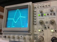
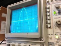
Here's the main difference I've seen between the two channels. This photo was taken while looking at the emitter of Q404:

There seems to be a large discrepancy between this (the bad channel) and the same signal located at the emitter of Q403:

Does this reveal anything to anyone? I'm about to break down and start removing all resistors and caps and measuring each one.
FWIW, I replaced all transistors back to the original transistors (with the exception of the output stage). This resulted in very little change, if any.
The signal shown above seems to be frequency, current, and temperature dependent. The higher the above three factors, the worse the distortion seems to get.
Any help appreciated!
Thanks!
Here's the main difference I've seen between the two channels. This photo was taken while looking at the emitter of Q404:
There seems to be a large discrepancy between this (the bad channel) and the same signal located at the emitter of Q403:
Does this reveal anything to anyone? I'm about to break down and start removing all resistors and caps and measuring each one.
FWIW, I replaced all transistors back to the original transistors (with the exception of the output stage). This resulted in very little change, if any.
The signal shown above seems to be frequency, current, and temperature dependent. The higher the above three factors, the worse the distortion seems to get.
Any help appreciated!
Thanks!
Attachments
Just FYI - never figured this out.
I literally replaced every cap and transistor on that channel and never made any progress.
Finally gave up trying to solve it... Just went with the fact that the issue really only shows up >10W at >15KHz, so it's not likely to show up in real-world listening.
With only a sample size of one, I don't know if the issue was with my board or with the design.
- Status
- This old topic is closed. If you want to reopen this topic, contact a moderator using the "Report Post" button.
- Home
- Amplifiers
- Solid State
- NAD 7225PE