It will work exceptionally well for the number of parts.
NFB is small, especially through crossover....
The auto-bias scheme scheme can be applied to more "evolved" designs, like the one proposed by John.
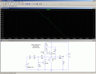
In this minimalist forms, it suffers from some minor deficiencies: although it does not suffer conventional crossover distortion, there are some "crossing artifacts" caused by the time taken by Q3 to get out of deep saturation.
Adding an antisaturation diode improves matters.
Using one or two diodes to reduce the swing seen by Q3's collector helps iron out the last residues.
Adding the diodes somewhat reduces the bullet-proof thermal ruggedness of the circuit, but even with two diodes, the voltage across the bases is bound to VD2+VD3-VD1, which means there is still ~1/2Vbe safety margin, quite sufficient for a "normal" environment.
Further sophistication is possible, to improve some parameters, like adding a second transistor to make the circuit symetrical, add B-E resistors, a holding capacitor, etc, but the circuit then loses some of its appealing simplicity.
Attachments
One thing I notice is that one output transistor never turns fully off.
The other turns completely off. If you add one NPN transistor, base
to base with Q2 and collector to collector with Q3. You get the AND
logic function (in current) from those series collectors. Unfortunately
it switches with some hysteresis and/or has no fuzzy threshold, but
it does permit both outputs a non-zero minimal current at all times.
With base to emitter resistors, you can further up current minimum.
Wish I could fuzz out that logic for a little bit smoother crossing.
Last edited:
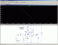
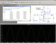
Even when ironing out the "wiggles" with all three diodes, HF distortion still isn't great. For a 28 mVp, 10 kHz input I'm getting like -28 dB 2nd. Not good "first (milli)watt" performance, I'd say.
A conventional 3-transistor, 2-diode circuit appears to be doing quite a bit better in this regard.
A conventional 3-transistor, 2-diode circuit appears to be doing quite a bit better in this regard.
In fact, it has little to do with HF: the behavior is similar at low frequency.Even when ironing out the "wiggles" with all three diodes, HF distortion still isn't great. For a 28 mVp, 10 kHz input I'm getting like -28 dB 2nd. Not good "first (milli)watt" performance, I'd say.
A conventional 3-transistor, 2-diode circuit appears to be doing quite a bit better in this regard.
As I said earlier, the audio quality is not very good, the H2 issue is caused by a gain change between the two situations: Q3 in linear mode/Q3 saturated.
This may look very surprising, but even used "backwards", Q3 provides some gain to the output.
Trying to follow the "gainy" signal path is an interesting intellectual exercise.
Anyway, there are possible workarounds.
The most obvious is to degenerate the negative half, see below.
B-E resistors can also be added to artificially raise the bias level, etc, etc
Attachments
Are you still there?
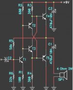
Here's a simple output stage I used for a tranny radio. Works well.
John
Hi John,
I particularly like your circuit for its simplicity and use of small transistors. Do you know the overall quiescent current drain please?
Should Q5 be mounted in contact with one of the output devices?
Regards,
currentflow
Looking at the schematic, quiescent current as shown should be about 9 mA (mostly VAS Ic) plus whatever you choose for the output stage. This circuit is on the low complexity side of things, so for decent performance it can't have super low current (one of the typical "pick two" situations).
It certainly can't hurt to mount Q5 like that.
It should be possible to add more output device pairs, but eventually compensation will be required.
It certainly can't hurt to mount Q5 like that.
It should be possible to add more output device pairs, but eventually compensation will be required.
Hi sgrossklass,Looking at the schematic, quiescent current as shown should be about 9 mA (mostly VAS Ic) plus whatever you choose for the output stage. This circuit is on the low complexity side of things, so for decent performance it can't have super low current (one of the typical "pick two" situations).
It certainly can't hurt to mount Q5 like that.
It should be possible to add more output device pairs, but eventually compensation will be required.
Thanks for your reply. I came to a similar conclusion when calculating the VAS current, which seems relatively high considering the amplifier's application, particularly if battery-powered. As you say, a compromise has to be made between current drain and performance.
Regards,
currentflow
One thing's for certain, these simple amps are quite fun to play with, at least in simulation. Add a pnp input stage and watch linearity improve considerably (thanks to higher loop gain no doubt). Take out bootstrapping and see it get worse.
Speaking of which: Can anyone explain what the "cost" of bootstrapping is here? I know it's a feedforward technique and the result is dynamically increased emitter resistance and hence VAS voltage gain and loop gain. But there has to be some kind of drawback, right? You obviously have to drive a few hundred ohms to supply so linearity into high-impedance loads may not be as good as it could be otherwise. But other than that? Higher output impedance?
Speaking of which: Can anyone explain what the "cost" of bootstrapping is here? I know it's a feedforward technique and the result is dynamically increased emitter resistance and hence VAS voltage gain and loop gain. But there has to be some kind of drawback, right? You obviously have to drive a few hundred ohms to supply so linearity into high-impedance loads may not be as good as it could be otherwise. But other than that? Higher output impedance?
Last edited:
Hi
Yes the VAS stage current is about 9 mA and I generally run the output stage bias at 5-10 mA.
It's a little higher than an equivalent Ge circuit (such as the 4 transistor one using driver and output transistors which might run at 5 mA total quiescen), unfortunately, but you could improve things with high gain Zetex transistors (e.g. minimum gain 200 or suchlike).
John
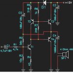
Nice evolution.
may be to try such a modification of scheme?
* - D1 is opened at negative half-wave output signal
and closes at the positive half-wave.
I am not sure this humble circuit deserves that attention
")
In addition, resistors around the circuit may improve the performances, but they will also require a well defined range of supply voltage to function properly, making the circuit less universal.
There are other possibilities, using a CCS instead of a bootstrapped resistor, changing Q3 for a NPN, etc...
Endless fun....
Of course: there are no free lunches in engineering:Speaking of which: Can anyone explain what the "cost" of bootstrapping is here? I know it's a feedforward technique and the result is dynamically increased emitter resistance and hence VAS voltage gain and loop gain. But there has to be some kind of drawback, right? You obviously have to drive a few hundred ohms to supply so linearity into high-impedance loads may not be as good as it could be otherwise. But other than that? Higher output impedance?
A composite of two transistors has a certain "figure of merit", in gain, transconductance, linearity, etc.
You can choose to allocate your resources in different ways, but basically the sum remains constant (except in really exotic topologies like Xquad).
The common collector stage has a total feedback; this has the advantage of a good linearity, but the total gain has to come from the previous CE stage.
By boostrapping the stage, you "unwind" some of the inherent feedback of the follower.
On the plus side, you get more gain from the EC stage, but you amplify the non-linearities of the BE voltage, you diminish the isolation from the load afforded by the common collector, etc.
In the very extreme, if you pushed the boostrapping to the maximum possible, you would revert to the performances of two CE stages cascaded: high gain, high distortion, high output impedance.
With the bootstrapping, you can choose a different trade off
I am not sure this humble circuit deserves that attention
You can draw a lot of simple circuits, it is trivial ...
However, to deal with the original scheme interesting!
Attachments
Good point re: load isolation. The increase in collector resistance afforded by bootstrapping obviously hinges on how close to unity EF voltage gain is. Any beta droop will thus also cause VAS gain (and loop gain) fluctuation and thus nonlinearity at high levels. TANSTAAFL indeed.
Sadly bootstrapping doesn't seem to be covered in standard textbooks very often. There's about one and a half pages in Horowitz/Hill (quite good, but not enough to cover the drawbacks we just discussed), but that's about it.
Sadly bootstrapping doesn't seem to be covered in standard textbooks very often. There's about one and a half pages in Horowitz/Hill (quite good, but not enough to cover the drawbacks we just discussed), but that's about it.
If you go for four transistors, try rather this one (with or without diode, with or without holding capacitor, and with a CCS it is even better)You can draw a lot of simple circuits, it is trivial ...
However, to deal with the original scheme interesting!
Otherwise, with your circuit you are attempting to tread on Edmond Stuart's patch
(I followed that path some years ago, it is interesting too, but in an other league)
Attachments
In the simple circuit I posted earlier, the bootstrap is preferred over a CCS because the voltage limit with a CCS is far too high for low voltage amplifiers. Usually the base of the CCS is fed from two diodes (Vf~1.3V) and this limits the collector to about 0.7V (approx. the voltage across the emitter resistor plus a Vce(sat). With a bootstrap the drive voltage can exceed the rail voltage.
FOr the same reason, actually the lower output half is limited as well because of the Vce(sat) of the VAS and Vbe(on) of the output PNP(s). To make sure you can achieve 1W it is necessary to use a double bootstrap. The 220 ohm bootstrap resistors should be replaced by 100 ohms, and a second bootstrap using 220 ohms added to the PNP base to ground line. The VAS collector is coupled into the TOP of the bias stabiliser.
It increases the bias current drain to about 20 mA but does give higher output powers before clipping.
Again if you want a really simple circuit which gives 1W the old germanium + dirver+output transformer designs were really quite efficient.
If you go to the trouble of using a double bootstrap it may be worth using high gain Zetex transistors to keep the quiescent current low.
John
Endless fun...
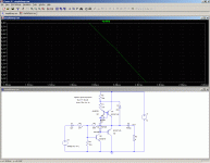
The transistor T3 in active mode and never goes into saturation.
Attachments
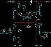
Hi Wakh
Your T3 is a Darlington and has a Vbe limit as a result! Also, the circuit would limit the negative swing becaue of Vce(sat) and Vbe(on) of the PNP.
I recommend a double bootstrap as the best option for low voltage amplifiers. This is about the only time I would suggest bootstrapping instead of CCS!
It really depends if you need 1W or can live with a little bit less...
John
- Status
- This old topic is closed. If you want to reopen this topic, contact a moderator using the "Report Post" button.
- Home
- Amplifiers
- Solid State
- Would like to build super simple mini transistor amplifier