Luxman used an IC in some of their otherwise excellent preamps that was unreliable. There were two actually, the DML-01 and the DML-02. This is about the latter, the DML-02. When these quit you are left with a boat anchor.
I have more anchors than boats so I'd like to clone this IC, but I need some help understanding the circuit so I can select some non-obsolete components. I'm semi-clever around tubes but not the hottest iron on the bench around solid state circuits, so this may involve a box of these: Just a warning, type slowly.
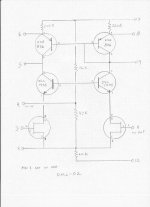
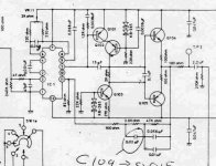
This site has a sketch of a circuit that might work but It uses lots of obsolete parts and I suspect that the pin 5 connection may have been inadvertently omitted (not sure). My C-12 amp has a replacement board that was probably a Luxman workaround once they figured out there was a reliability issue with the potted IC so I removed it and drew it. That drawing is attached. It's similar but uses only six active devices rather than eight.
I have intentionally left the bottom pair of devices ambiguous as I am not sure what they are; no marks on the devices (all TO-93). Looking at the other drawing, they are probably a 2SK60 which is some sort of FET that I am not familiar with - and since I don't really get the circuit, I'm leaving it that way until I am a bit smarter about it.
I'm hoping to get some input on how the circuit works and some thoughts on substituting modern devices. Perhaps dual devices would make sense.
One more note on that drawing. The first two pairs are symmetrical but the third (mystery pair) are not. By that I mean that the drain will be at the top on one and the bottom on the other.
I have more anchors than boats so I'd like to clone this IC, but I need some help understanding the circuit so I can select some non-obsolete components. I'm semi-clever around tubes but not the hottest iron on the bench around solid state circuits, so this may involve a box of these:
Just a warning, type slowly.This site has a sketch of a circuit that might work but It uses lots of obsolete parts and I suspect that the pin 5 connection may have been inadvertently omitted (not sure). My C-12 amp has a replacement board that was probably a Luxman workaround once they figured out there was a reliability issue with the potted IC so I removed it and drew it. That drawing is attached. It's similar but uses only six active devices rather than eight.
I have intentionally left the bottom pair of devices ambiguous as I am not sure what they are; no marks on the devices (all TO-93). Looking at the other drawing, they are probably a 2SK60 which is some sort of FET that I am not familiar with - and since I don't really get the circuit, I'm leaving it that way until I am a bit smarter about it.
I'm hoping to get some input on how the circuit works and some thoughts on substituting modern devices. Perhaps dual devices would make sense.
One more note on that drawing. The first two pairs are symmetrical but the third (mystery pair) are not. By that I mean that the drain will be at the top on one and the bottom on the other.
Attachments
Last edited:
Are you sure that drawing is correct ? As it is I can´t see what it is supposed to do.
If the bottom pair is unknown how do you know that they are not both connected with
their sources to the 22k resistor ?
If I change some connections I could imagine a working cascoded differential amplifier:
The two 2SA836 form a current mirror as they are connected.
The two 2SC1435 could be for cascoding. In this case their bases must be connected to the point where the 56k and 47k resistors meet (pin4)
The two FETs would be connected with their sources to the 22k resistor which then provides the current through them.
Then the gates of the FETs would be the inputs and pin 5 and 9 the outputs of a differential amplifier.
Are you sure that drawing is correct ? As it is I can´t see what it is supposed to do.
If the bottom pair is unknown how do you know that they are not both connected with
their sources to the 22k resistor ?
Oh Yeah!! That drawing is WRONG! There should be a node in the center of that drawing. The junction of the 56K and 47K resistors happens at pin 4.
As for your other points, all I can say with any authority is that these devices are in TO-92 packaging and that the pin numbers on the drawing are correct. I only think that they are FETs because of the similarity to the other drawing. I can't know with any certainty how the FETs are connected within the TO-92 package. I'll think about what you have said about the FETs
I used a scope and a signal generator to study both the one existing (still working) encapsulated IC and this workaround part. They seem to function the same and the notes about the pin 4 input and pin 11 output are correct.
The link I posted in the IP has a schematic of the entire circuit so that one can see how the IC works within the larger circuit.
Last edited:
But something must be wrong, the gate of a FET can´t be an output.
http://www.hilberink.nl/codehans/luxdml2.jpg (The picture "Below the schematic diagram of the DML-02") shows what I have just described, except that instead the 22k resistor there is an active current source.
Ah now I see (in the complete schematic) pin 11 is the negative _input_. You can measure the output signal on pin 11 because the feedback loop is connected there.
Ok I think we make progress I´ll look into the details tomorrow (it´s already evening here in europe) and post schematic.
http://www.hilberink.nl/codehans/luxdml2.jpg (The picture "Below the schematic diagram of the DML-02") shows what I have just described, except that instead the 22k resistor there is an active current source.
Ah now I see (in the complete schematic) pin 11 is the negative _input_. You can measure the output signal on pin 11 because the feedback loop is connected there.
Ok I think we make progress
I´ll look into the details tomorrow (it´s already evening here in europe) and post schematic.OK, I'm beginning to understand the circuit a little better now. But if this is a cascode circuit, as it appears, then looking at the right side of the drawing, the input would be to the base of the lower BJT (pin 4) as it is, but the signal out should come from pin 8. I'm thinking here of an analogy to the tube cascode circuit where the input is from the grid of the lower triode and the output is from the plate (anode) of the top triode. But I can't see than being correct within the context of the larger circuit.
I suppose the purpose of the bottom two FETs is to hold a constant DC voltage on the emitters of the lower BJTs in the cascode. Have I got that much right?
The top rail runs at 29 volts. Everything else is at a lower voltage.
I suppose the purpose of the bottom two FETs is to hold a constant DC voltage on the emitters of the lower BJTs in the cascode. Have I got that much right?
The top rail runs at 29 volts. Everything else is at a lower voltage.
The top rail runs at +29.5 and the bottom rail runs at -29.5.
So pin 7 runs at the top rail voltage.
6 and 8 at 29.3
5 at 28.8
4 at 13.7
3 and 11 at zero
2 at 0.5
I put a small signal into the phono stage and set the volume contol for 200mv at the output. Then I measured signals on the 2,3,4 and 11. 4 showed 16.6 mv and 2, 3 and 11 showed 30 mv.
I can now say with a great deal of confidence that I definitely don't understand this circuit
the notes about the pin 4 input and pin 11 output are correct.
No, that should be pin 3 input and 11 output. Note that pins 2 and 4 are only a .001uf cap that bypasses the 47K resistor. Nothing else going on there.
Last edited:
Throw in my 2 cents - since this is part of a circuit, not the whole circuit, the closest to an output would be pin 9, which should go to the next stage of the circuit. AC wise most of the pins should have close to same signal as the input. The top 2 transistors form a current mirror, the middle pair are cascoded to the input pair of FETs. Someone on the previous thread mention 2sk68 which are probably what the FETs were, not 2sk60. Pin 9 is the only pin with a lot of ac gain, but still don't expect to see large signals.
Pin 3 and 11 would be non inverting and inverting inputs - feedback would be fed into 11 if 3 is input. Pin 9 should have highly amplified Difference between pins 3 and 11.
Pin 3 and 11 would be non inverting and inverting inputs - feedback would be fed into 11 if 3 is input. Pin 9 should have highly amplified Difference between pins 3 and 11.
Last edited:
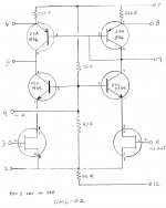
The schematic in #4 seems to be correct, it should work and make sense
if you look at it in context with the rest of the circuit (see attachment).
pin 3 is + Input, pin 11 is - Input (where the feedback loop is connectet).
pin 5 is the output from the differential amplifier and goes to the voltage
amplification stage.
if you look at it in context with the rest of the circuit (see attachment).
pin 3 is + Input, pin 11 is - Input (where the feedback loop is connectet).
pin 5 is the output from the differential amplifier and goes to the voltage
amplification stage.
Attachments
From your measurements in #8 we can calculate a current
of approx. 0.8 mA through each leg of the LTP, this makes
me believe that the FETs are most likely low Idss types.
Probably some low noise Toshiba GR type.
A matched pair of 2SK170GR should do it. Or if you want
them factory matched (which I would prefer) a LSK389A :
http://www.linearsystems.com/datasheets/LSK389.pdf
In any case the sources of both FETs should be connected
to pin 2. (I have read that some Toshiba FETs were symmetrical
and could be mounted "upside down", but I would rather not experiment.)
For the bipolar resistors any current production low noise
small signal BJT should work. Examples:
2SA836 -> 2N4403, BC560C
2SC1445 -> 2N4401, BC550C
OK. I didn't see this as a long tailed pair until now. Those are common enough in vacuum tube circuits. I looked for a signal on pin 5 and didn't see any but I will go back later today with the scope and have another look.
The wiki article on differential amplifiers has a drawing very similar to this circuit labeled as figure 3 HERE, which I stumbled upon reading about current mirrors. I'm going to have more questions but I'll ponder this first.
It occurs to me that the function of this circuit is to sum in the feedback with common mode rejection. Is that your take or is there more to it?
Do you think I have the gate, source and drain labeled correctly on my drawing or do I have the source and drains inverted?
Thanks for your help with this, Georg, Homemodder and Steve.
Last edited:
most likely low Idss types.
NEC 2SK68 came in 4 Idss grades ; 0.5-1.5 mA, 1-3 mA, 2-6 mA, 4-12 mA.
(pleasure of having various oldy Japanese small signal semi databooks)
Other possibility for the 2SK60 slip-up in the schematic could have been a 2SK61-0, 1-3mA Idss grade. Very unlikely though, doesn't have a pretty noise figure.
Attachments
Good find! How did I miss that one?
And I'm in luck! I pick up my mother-in-law tonight. How is that luck you ask? She's a Japanese national. I bet she can translate that blog. Perhaps there will be a source for those PCBs.
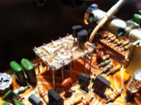
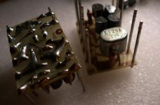
As you can tell from the photo, that is the same board but with a different device. Pin one is at the front of the image on the right side of the photo, to the left of the device labled K129A. That probably makes the K129A a dual FET.
I'll have to look into the specs on that K129A. The solder job is much better on that board too. The devices on mine may not be the original.
And I'm in luck! I pick up my mother-in-law tonight. How is that luck you ask? She's a Japanese national. I bet she can translate that blog. Perhaps there will be a source for those PCBs.
As you can tell from the photo, that is the same board but with a different device. Pin one is at the front of the image on the right side of the photo, to the left of the device labled K129A. That probably makes the K129A a dual FET.
I'll have to look into the specs on that K129A. The solder job is much better on that board too. The devices on mine may not be the original.
Last edited:
the specs on that K129A.
Is dual K68A in a metal can (similar deal as Toshiba K146 and K147)
- Status
- This old topic is closed. If you want to reopen this topic, contact a moderator using the "Report Post" button.
- Home
- Amplifiers
- Solid State
- Cloning the Luxman IC known as DML-02