reverse-ingeneering the PA0016
Most likely the PA0016 IC is based on this patent: Push-pull amplifier
However, this patent contains a serious error: the connection between node 'P' and 'out' gives an enormous amount of distortion. This is because it violates the 'crosswise connection rule'. Why does Pioneer apply for such a patent? To mislead the competitors?
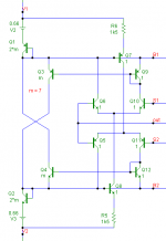
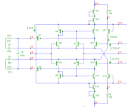
In the meantime I've tried to reverse-engineer this chip, see 2nd picture. This one does a reasonable job.
(notice the multiplier m=7 !)
Cheers,
E.
edit: @ homemodder, our posts just crossed.")
It is similar with voltage feedback type, interesting is that batteries between pin8-pin9 and pin13-pin14, that gives direct driving from VAS to OPS.
Most likely the PA0016 IC is based on this patent: Push-pull amplifier
However, this patent contains a serious error: the connection between node 'P' and 'out' gives an enormous amount of distortion. This is because it violates the 'crosswise connection rule'. Why does Pioneer apply for such a patent? To mislead the competitors?
In the meantime I've tried to reverse-engineer this chip, see 2nd picture. This one does a reasonable job.
(notice the multiplier m=7 !)
Cheers,
E.
edit: @ homemodder, our posts just crossed.
Attachments
Last edited:
Yes, that was the patent.
No, may be that is not wrong connection, if it has correct values, it help canceling error, because their non switching gives more drop voltage that need to be canceled. While without it, is just variable Vbe mult. I am going to try with it to check it out.
No, may be that is not wrong connection, if it has correct values, it help canceling error, because their non switching gives more drop voltage that need to be canceled. While without it, is just variable Vbe mult. I am going to try with it to check it out.
Last edited:
PA0016
Indeed, there are (too) many differences. Let's forget this patent, as it only puts us on the wrong trace. At first sight, I (wrongly) thought that the circuit was powered by the VASes (or VAS+CCS). That's not the case: it's powered by the main supply rails. For the same reason, please, also forget my comment about "the connection between node 'P' and 'out'" .
Indeed, there are (too) many differences. Let's forget this patent, as it only puts us on the wrong trace. At first sight, I (wrongly) thought that the circuit was powered by the VASes (or VAS+CCS). That's not the case: it's powered by the main supply rails. For the same reason, please, also forget my comment about "the connection between node 'P' and 'out'" .
Last edited:
Yes, that p (as 3rd input) is not connected at the IC pin4, I just thought that it doing some EC, but actually not like that.
Ok forget that big drop circuits. I just only interested at its independent bias controlling. Also there should any I-sense voltage limiter that not present. BTW, thanks for your reverse engineering.
Any news from AB2?
Ok forget that big drop circuits. I just only interested at its independent bias controlling. Also there should any I-sense voltage limiter that not present. BTW, thanks for your reverse engineering.
Any news from AB2?
Last edited:
reverse-ingeneering the PA0016
Hi Homemodder,
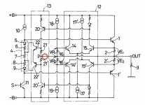
See: Emitter-follower type single-ended push-pull circuit - Pioneer Electronic Corporation
Funny enough, I've downloaded this patent several years ago, but I didn't realize it was about the PA0016 chip from Pioneer AND about Class-I
[size=+2]The PA0016 is Class-I ![/size]
Sure. The 1st picture is a copy from the patent, the 2nd one is my attempt of reverse engineering.
Pin 4, the class-i input, isn't used in every Pioneer amp, but in the A-91D, for example, it is used. As a result, quite a low level of distortion: 0.003% @ 20Hz...20kHz.
Cheers,
E.
[snip]
Type 2 was improvement on this scheme but I haven't been able to locate its patent as yet.
Hi Homemodder,
See: Emitter-follower type single-ended push-pull circuit - Pioneer Electronic Corporation
Funny enough, I've downloaded this patent several years ago, but I didn't realize it was about the PA0016 chip from Pioneer AND about Class-I
[size=+2]The PA0016 is Class-I ![/size]
[snip]
Edmond do you have the schematic of the circuit ??
Sure. The 1st picture is a copy from the patent, the 2nd one is my attempt of reverse engineering.
Pin 4, the class-i input, isn't used in every Pioneer amp, but in the A-91D, for example, it is used. As a result, quite a low level of distortion: 0.003% @ 20Hz...20kHz.
Cheers,
E.
Attachments
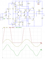
That was with the help of a upgraded power supply as the original is not up to the task and sags terribly. The design of the amp, three gain stages already provide very low distortion even without the err correction nonswitching circuitry.
The A91D in literature is referred to as a TYPE 3 nonswitching amplifier, although it seems the same chip is used as TYPE 2. Looking at a few amps that use this chip one notices that the models using it without the pin 4 connection claim the same THD20 figures as the models using pin4.
The A91D in literature is referred to as a TYPE 3 nonswitching amplifier, although it seems the same chip is used as TYPE 2. Looking at a few amps that use this chip one notices that the models using it without the pin 4 connection claim the same THD20 figures as the models using pin4.
So, type 2 and type 3 has same IC, the different is just pin4 connected or not connected, like that? Type 1 is that with big drop? (means less linear than if without it / bigger drop).
From the prior art fig1, it should leads to AB2, not voltage feedback (or they called it type 2&3). Also there is kendall type called class i.
From the prior art fig1, it should leads to AB2, not voltage feedback (or they called it type 2&3). Also there is kendall type called class i.
>I see no differences within kendall's and nakayama's type.
I don't see it either. See also: http://www.diyaudio.com/forums/ever...-linear-audio-publication-41.html#post2799107
I don't see it either. See also: http://www.diyaudio.com/forums/ever...-linear-audio-publication-41.html#post2799107
May be this one is better than old version of non feedback pioneer's, 0.1V drop voltage for normally 1V drop without it, no feedback (input compared FB).
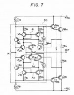
Found it at AR D400 and may be soulution I don't really know for this. I search for any patents and negative.
Found it at AR D400 and may be soulution I don't really know for this. I search for any patents and negative.
Attachments
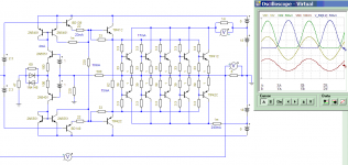
If I understand correctly, the six transistors at the left side provide error cancellation (to a certain extent). However, this part of the circuit is output voltage controlled whereas the actual needed amount of error cancellation depends on the output current. So this compensation scheme works only as intended with a fixed resistive load.
While I obsessed upon Schottky diodes being the only devices to switch off,
there are stability advantages to letting the common mode feedback devices
turn off. Its a real pain to compensate two loops that interact nonlinearly,
even at 90deg.
I think Edmond's way (and Elvee's cirlophone way) are better ideas, even
if transistors in the common mode loop are regularly turning off. Its not in
the differential loop where you would hear it. The mixing of compensations
is far less messy when you allow for the shutoff.
Last edited:
It is load dependent, but it smoothen crossover distortion to a level that could be reduced with negative feedback that normally has slow response. Also its load dependent is not harmful, may be with mosfet like in AR D400, or more diode arrangement, it has better smoothening result. Soulution 710 gets very low THD <10ppm without NFB, don't really know what they mean with without feedback.
Attachments
The failing of that one is the same as every ordinary AB emitter follower.
Nonlinear common mode feedback is shaped by output devices that are
not at constant temperature. Sims may not reveal the obvious here.
Even you compensate some desired non-linearity beforehand, those
hot output devices (and also load impedance) are not to be trusted.
Common mode negative feedback (aka quadrature feedback in other
threads). Even ordinary AB amps with a sliding bias of fixed voltage
already have this. Its actually a concept we are already familiar with.
Something sets output quiescent current, emitters and resistors, else
it runs away! But the braindead way this is usually handled is neither
temperature independant, nor produces the desired non-switching.
All the good circuits use supplemental devices of oversized thermal mass
and low dissipation to monitor the true currents, and make well informed
decisions about how to shape bias for ideal current non-linearity. Hopefully
to make gentle non-switched crossings with any load. Output devices that
do hot work are not permitted to participate in decisions about current.
Last edited:
well.. if nonswitching target is thermal stability, thermally coupled NTC/PTC or diode is the best, because it does not affecting amplifier performance at all.
That I like from this technique is it canceling crossover distortion, not rejecting, or reducing by NFB. Principle of 2 diode crossover gap (mosfet in AR D400) added to input to cancel crossover distortion of output.
for canceling principle:[ error - error = eliminated ] then, [ crossover distortion - crossover distortion = no crossover distortion ].
- Status
- This old topic is closed. If you want to reopen this topic, contact a moderator using the "Report Post" button.
- Home
- Amplifiers
- Solid State
- Class i and siblings