Hi,
I designed, built, tested and listened to this amplifier. Its circuitry is a bit different, but I find it sounds very good (very difficult to tell it apart from a tweaked Linn amp using blind, level-matched AB switching), and it does not generate the excessive heat from a class A design.
Its design is based on a non-complementary BJT circuit. It runs
class AB, and uses current amplifying stages instead of voltage
amplifying stages (VAS) to drive the output transistors. The output
stransistors are in a totem-pole configuration, but run common
emitter rather than the usual common collector (emitter follower)
layout. The front end of the amplifier uses a differential compound
pair (Sziklai).
The first transistor after the differential pair is biased such
that instead of cutting off sharply for class AB, it has an
extended non-linear cutoff to minimize the impact of "crossover"
distortion. This base circuit also compensates
for the inherent non-linearity of the "gm doubling" of the output
transistors when run class AB. The result is that over the entire
operating range, the openloop gain of the amp doesn't vary more than
5-10%. Closing the feedback loop with about 60db of loopgain results
low distortion.
measurements using +21/-21 volt power rails:
Output power (.003% distortion) 35 watts @ 4 ohms
output power (.1% distortion) 45watts @ 4 ohms
freq. response: 10Hz-50KHz +0-3db
Low freq. limit set by coupling capacitor, can be eliminated for DC
Slew rate: 5V/us (can be increased but requires 10uh in parallel with 10
ohms in series to load)
Capacitive loads: stable (with 2V/us slew rate) with 1uf low-ESR load.
Distortion (@ 1khz): 2nd harmonic below -90db for 35 watts or less
3rd harmonic below -85db for 35 watts or less
higher harmonics below -90db for 35 watts or less
Output stage protection: output voltage diode clamped to rails
output current limited to 4 amps after 10ms
DC on output: adjustable to zero, stable to a few millivolts.
I enclosed the schematics and an LTSpice ".asc" file to show the gain linearity while the input is DC swept. Plot the derivative of the output voltage "d(V(Vout))". The circuit requires the Cordell models for MJL3281, 2N5089, 2N4403. I have used MPSA56 transistors extensively, and the SPICE model is on the ON Semiconductor site, or just use 2N4403's instead. MPSA56's were popular 'cause I had a whole pile in my transistor bin.
The circuit is a bit of a fluke.... it originally was a class A design - one of the design iterations showed better performance running class AB! You can probably greatly increase the power output with higher voltage rails. I didn't need much power, and I had a pair of transformers scavenged from a few cheapy UPS's that would only do 21 volts DC.
Feel free to use the circuit as you wish, please tell me if there's anything you think that might improve its sound.
Paul G.
Attachments
I'm probably not clever enough to pick up on the subtleties of your overall circuit.
What I see is a dual VAS that has been cascoded. The VAS directly drives the output devices. What's special about that?
Do you have sufficient current gain to drive a load? Particularly a speaker load.
The +IN base sees 110k, the -IN base sees 9k1.
I suspect you have to deliberately unbalance the input LTP to cancel out the input offset current and voltage and thus achieve near zero output offset.
Last edited:
+ 1 on Andrew’s comments. About the only thing I see atypical about the circuit is the output stage bias feedback. One thing you could try doing is connecting the RC’s of C100 and C200 to the collectors of the 2nd stage cascodes instead of the collectors of the VAS’, may be able to run a lower value of C that way, possibly upping the slew rate. Just a thought, I'm sure you've worked a lot of angles of the design.
The output devices are current driven to give voltage translation from the positive rails, and to ignore the effect of the very different base voltages of the output transistors. The current drive allows the output transistors to both run at full gain - there is no feedback as you'd get with an emitter follower, since the base currents are unaffected by the emitter voltages. The cascoding of the driver transistors (Q100,Q200) ensures that the currents remain balanced despite the difference in pwr transistor bases.
The "magic" is in the 470 ohm (R100, R200) base circuit for Q100, Q200. The voltage across that resistor is developed by the input differential circuit. That voltage causes Q100 and Q200 to create collector currents, but the base voltage to collector current relation is non-linear (exponential). As the base drive comes from higher impedance, it becomes more of a current drive, and as such becomes more linear. In effect, you can control the degree of non-linearity of a transistor common emitter stage by the Thevenin resistance of the base drive. In this case, for a 400-500ma output transistor bias current, the value of R100, R200 seems to balance the non-linearity caused by the output transistors and gm doubling.
If I replace the 470 ohm R100, R200 by a high impedance active load, there is a kink as both output circuits go into conduction, and the gain doubles as you'd expect in gm doubling. Note that gm doubling is much reduced in an emitter follower - as you'd expect when you apply the feedback formulas. Using the 470 ohm resistor gives an open-loop gain variation of 5-10% over the full range, compared to a greater than 2:1 variation when using a more conventional circuit. For a given bias current, there is an optimum value of R100, R200.
I have some trouble trying to explain WHY this works, and how to predict the optimum values for R100,R200. During best linearity, it turns out that Vbe of the driver transistor matches Vbe of the output transistor over the full signal range, within a few millivolts. I am not sure what that signifies. Also, the optimum linearity occurs when R100,R200 are approximately the dynamic value of rbe for Q100,Q200.
The other wrinkle is that the non-linearity allows a very gradual cutoff as the output transistors shift out of class A operation. It's very difficult to measure the precise cutoff point, and I don't see any bumps or nicks as the circuit transitions through cutoff. Measuring distortion at lower signal levels is quite difficult, since my equipment is limited to about -105db distortion. There was nothing I could see. I am relying on measured results, not simulated ones. I find that LTSpice did not give me results that were close in the case of distortion limits or high frequency stability, but its good enough to see what direction to go in.
There is definitely enough gain to drive a speaker. The open loop gain of the circuit is about 2000-3000, as computed by LTSpice. When the feedback loop is closed the gain is 10, giving me a loop gain of 200-300, or about 50db. Because of the better linearity, I can use less feedback, and still get overall distortion products of about 90 db below full output.
The driver transistors can supply 50-100ma into the MJL3281 bases. The output transistors have an Hfe of 150, yielding 8-15 amps. That is more than enough current for a 35 watt amp. The limiting circuit will allow high current transients, but will pull back when the average transistor current is greater than 4 amps. The speaker sees twice the current variation for each power transistor.
The amp has inverting type feedback, so the input impedance is about 10k in parallel with R2 (100k). If you make the reasonable assumption that the main input is driven by a voltage source, both bases of the differential pair see about 9.1kohms AC impedance. You are correct at DC conditions. On the other side of the diff input, I should put a 4.7uf cap in series with R13 (9.1k), and add a DC path to ground, about 51 Kohms. That should improve the DC stability and the AC balancing. During the beginning part of the design I didn't use a coupling capacitor, and ran everything DC. That caused a few problems with some signal sources, so the capacitor went in, and I neglected to match the DC circuitry. Thanks for the tip!
By the way... the reference designators (Q100, R200, etc) I mention are from the PDF files I attached above. The LTSpice circuit has quite different reference designators.
Paul G.
I will need to read your technical method of operation a few times to understand the working..........The driver transistors can supply 50-100ma into the MJL3281 bases. The output transistors have an Hfe of 150, yielding 8-15 amps.
But look at the datasheet. There is no way hFE=150 when output current = 15Apk
BTW,
45W into 4r0 would require a peak current capability of ~15Apk without much loss of output voltage, to make it capable of driving a 4ohm reactive speaker for all types of music.
There is no point in testing to see if the amplifier can deliver 15Apk into 0r1. That is quite different.
+ 1 on Andrew’s comments. About the only thing I see atypical about the circuit is the output stage bias feedback. One thing you could try doing is connecting the RC’s of C100 and C200 to the collectors of the 2nd stage cascodes instead of the collectors of the VAS’, may be able to run a lower value of C that way, possibly upping the slew rate. Just a thought, I'm sure you've worked a lot of angles of the design.
That would defeat the isolation that the cascode stage gives. Notice that both power transistors are NPN, and one emitter is close to the output voltage, and the other emitter is at the negative rail. One set of cascode collectors has about .5v AC, the other one can vary almost from +rail to -rail. Although at first glance it looks like a complementary emitter follower circuit, it really is two stacked common emitter transistors. The current drive from the cascode forces the same gain from each power transistor.
Without the cascode isolation, signals from the upper power transistor will feed back and unbalance the drivers.
I tried moving the compensation circuit around (it creates a dominant pole), stability seemed best where it is now. It seemed that setting the open loop -3db freq. response to about 8kHz would give stability. The closed loop response is between 50-100KHz. There are two other compensation circuits (R54-C53, R12-C5), they were necessary to keep things stable with a 1uf across the load, running flat out.
I chose a slightly slower more stable amp instead of a faster one with the R-L (10 ohm in parallel with 10uH) in series with the output.
Paul G.
I've gotta say, a pretty design ") Effective use of cascodes and I like the current based gain mechanism, essentially you're turning the output devices themselves into a VAS. Also the parallelling of cascode devices is a nice way to disperse power.
Effective use of cascodes and I like the current based gain mechanism, essentially you're turning the output devices themselves into a VAS. Also the parallelling of cascode devices is a nice way to disperse power.
The only comment I have that might improve your figures is to lower the feedback resistance, if you can/want to afford a lower impedance input. I think it'd help reduce noise figures.
Is it correct that the bias adjust has to be a multiturn for any sensibly accurate Iq adjustments?
Effective use of cascodes and I like the current based gain mechanism, essentially you're turning the output devices themselves into a VAS. Also the parallelling of cascode devices is a nice way to disperse power.The only comment I have that might improve your figures is to lower the feedback resistance, if you can/want to afford a lower impedance input. I think it'd help reduce noise figures.
Is it correct that the bias adjust has to be a multiturn for any sensibly accurate Iq adjustments?
There appears to be a common mode loop, Q8 acting on the sum of the voltage drop across R50/51. This loop goes back to Q1, modulating the value of the CCS. I've used the same basic concept to bias a VAS, but not including the output stage. Interesting way of biasing quasi output stage.
BTW, J-fets are nice too, especially for CCS.
BTW, J-fets are nice too, especially for CCS.
I've gotta say, a pretty design
The only comment I have that might improve your figures is to lower the feedback resistance, if you can/want to afford a lower impedance input. I think it'd help reduce noise figures.
Is it correct that the bias adjust has to be a multiturn for any sensibly accurate Iq adjustments?
I haven't noticed any noise issues - 2N5089's are pretty good for noise, and the AC impedance of the base circuits is around 9kohms. Looking up the specs for 2N5089, it claims less than a 2db noise figure for the audio band. We live in a very quiet area, and I haven't heard any noise while listening to the amp. Putting my ears about 2 inches from the speaker, I can hear a bit of 120Hz, but no hiss. At a foot or two distance I can't hear anything. The speakers are PSB Stratus Gold's. With horns or more efficient speakers you might be able to hear it close up.
It doesn't need any fancy 10 turn pot for bias adjustment. I use a single turn trimpot, and I use either an ammeter or the bi-colour LED circuit shown in the optional circuits above. Changing the output stage's current while monitoring the distortion shows a broad minimum of distortion. Setting the current plus or minus 100 ma from the 400ma optimum changes the distortion by one or two db.
What really messed up the distortion was when the circuit oscillated at several MHz. The RF would not show up at the output (except as distortion as it changed amplitudes). Even with a 100 MHz 'scope, the RF amplitudes were barely visible, and they'd change depending on the audio signal. Once the circuit was properly compensated, a lot of distortion and sporadic RF disappeared.
Paul G.
There appears to be a common mode loop, Q8 acting on the sum of the voltage drop across R50/51. This loop goes back to Q1, modulating the value of the CCS. I've used the same basic concept to bias a VAS, but not including the output stage. Interesting way of biasing quasi output stage.
BTW, J-fets are nice too, especially for CCS.
It takes about 2 amps through R50-R51 before Q8 begins to conduct. This is the overcurrent control. C12 smooths out the waveform so that the overcurrent reacts to average output current. (With a sine wave output, the voltage across R50-R51 appears as a rectified sine wave)
The operating point is controlled by the current source in the long-tailed pair. It's quite stable, and D5,D6 are mounted on the transistor heatsinks to keep things from getting too hot. Just to be sure, I ran both channels full out into a short circuit, and let it cook for about 20 minutes. Once the shorts were removed, the bias current was maybe 100ma lower than it should have been, until things cooled down.
Paul G.
Hi,
I designed, built, tested and listened to this amplifier. Its circuitry is a bit different, but I find it sounds very good (very difficult to tell it apart from a tweaked Linn amp using blind, level-matched AB switching), and it does not generate the excessive heat from a class A design.
Its design is based on a non-complementary BJT circuit. It runs
class AB, and uses current amplifying stages instead of voltage
amplifying stages (VAS) to drive the output transistors. The output
stransistors are in a totem-pole configuration, but run common
emitter rather than the usual common collector (emitter follower)
layout. The front end of the amplifier uses a differential compound
pair (Sziklai).
The first transistor after the differential pair is biased such
that instead of cutting off sharply for class AB, it has an
extended non-linear cutoff to minimize the impact of "crossover"
distortion. This base circuit also compensates
for the inherent non-linearity of the "gm doubling" of the output
transistors when run class AB. The result is that over the entire
operating range, the openloop gain of the amp doesn't vary more than
5-10%. Closing the feedback loop with about 60db of loopgain results
low distortion.
Paul G.
Is there not a great similarity to the circuits about follow URL's
http://www.diyaudio.com/forums/solid-state/162644-siliconix-siemens-nmos-amplifiers.html
http://www.amplimos.it/images/2sk77 amp YAMAHA B-1.gif
http://www.amplimos.it/images/2SK1056AMP.bmp
http://peufeu.free.fr/audio/schemas/Kaneda_Mosfet.jpg
‹à“cŽ®_UHC_MOS-FET_Power_Amp
(except the fact, that there are MOSFETs in the output stage in use instead BjT) ??
more URLs you will find by 1) (by post #1) about
http://www.diyaudio.com/forums/soli...better-audio-non-complements-audio-power.html
Last edited:
Is there not a great similarity to the circuits about follow URL's
http://www.diyaudio.com/forums/solid-state/162644-siliconix-siemens-nmos-amplifiers.html
http://www.amplimos.it/images/2sk77 amp YAMAHA B-1.gif
http://www.amplimos.it/images/2SK1056AMP.bmp
http://peufeu.free.fr/audio/schemas/Kaneda_Mosfet.jpg
‹à“cŽ®_UHC_MOS-FET_Power_Amp
(except the fact, that there are MOSFETs in the output stage in use instead BjT) ??
more URLs you will find by 1) (by post #1) about
http://www.diyaudio.com/forums/soli...better-audio-non-complements-audio-power.html
I always enjoy following down your many references to posted circuits. The closest one is the Siemens/Siliconix circuit although it uses MOSFETs. I did use MOSFETs in one of the earlier versions of the circuit I posted, but I could not get the low distortion that the BJT gave me, especially after adding curvature to the transfer characteristics (using Q100,Q200). Looking at the circuit values, I believe all the designs you posted do not deliberately use non-linearity to compensate for gm-doubling and get a "soft" transfer between class A to AB.
I would not be at all surprised if the technique I use is already patented - I have made up circuits like class D amplifiers, and discovered what I thought was new, is really a well beaten path.
The topology I used isn't really all that new. The only thing I haven't seen done before is the trick using the non-linear Vbe-Ic relation to reduce distortion. I tried using the same trick with MOSFET output devices, but I could not get the same low distortion, unless I used ton's of feedback (with the usual HF stability problems). It's actually quite easy to convert my circuit to MOSFET, just run the cascodes into a resistor between gate and source, and adjust biases.
My circuit doesn't really show itself off as being all that unusual. However - I'm quite pleased with its performance. I'll probably be tearing it apart in a few weeks time to try something else! Right now it's on a "special" breadboard with nice big heatsinks and a hefty power supply. The circuit you see is about the hundredth iteration using LTSpice, and about the fifth physically built since this spring.
Anyhow... thanks for your references!
By the way, I rarely see amplifiers that use inverting input feedback, where the first stage has signal and feedback coming together on the same node. This gives some problems with input impedance, but I can't see any other disadvantage. Is it a technique frowned-upon by audiophiles?
Paul G.
The Circlophone uses a similar trick, at Q9/Q11's level, with the 56Ω B-E resistors driven in current mode by the VAS:The topology I used isn't really all that new. The only thing I haven't seen done before is the trick using the non-linear Vbe-Ic relation to reduce distortion. .
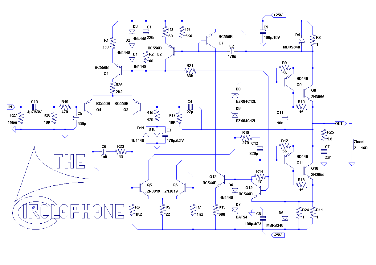
But the Circlophone does not only rely on that mechanism to shape the crossover: subtraction of exponentials cannot yield a perfectly linear function, and the "best fit" region is very narrow.
These two issues are addressed by the common-mode servo: it keeps the open-loop transfer function at the optimum bias point and then straightens it further in real time.
Our amplifiers have similar topologies, the stages are arranged somewhat differently though.
I have found that a cascode in front of the OP stage brings no benefit.
This might look counter-intuitive, but I recommend you try to bypass them, you might be surprised.
Yes, you are right. This models I know:Anyhow... thanks for your references!
By the way, I rarely see amplifiers that use inverting input feedback, where the first stage has signal and feedback coming together on the same node. This gives some problems with input impedance, but I can't see any other disadvantage. Is it a technique frowned-upon by audiophiles?
Paul G.
1) AVM
for basic schematic go to post #4 about
http://www.diyaudio.com/forums/soli...ody-burmester-avm-schematics.html#post2598494
more URLs:
http://www.diyaudio.com/forums/solid-state/27644-stereoplay-1988-monoblock-guenter-mania.html
Wer kennt sich mit AVM Verstärkern aus?, Verstärker/Receiver - HIFI-FORUM
anywhere on this forum I have post the simulation results of this topology
2) the first amp designs (e. g. 101, 105) from Bob Stuart & Allen Boothroyd (Meridian Audio) uses the inverted modes
dhs Meridian 101 Control Unit
Meridian 101 experts: Help needed! - pink fish media
MERIDIAN INTERGRATED AMPLIFIER MCA-1 BOOTHROYD AND STUART LTD FAULTY | eBay
Beyond The Wall Of Sleep: Meridian Boothroyd Stuart 101/105 Schematics & Fault Finding Guide
There was also an paper from Bob Stuart & Allen Boothroyd, where this was justified in detail, but I can't find it.
3) Musical Fidelity A1-X (only preamp line section and RIAA head amp - go to the attachement)
BTW - low input impedance between 1K and 5K is an advantage and not a disadvantage (at least by modern op amp ICs and discrete line amp solutions). Parasitic lead (cable) effects are less critical. Only in cases of tube preamp line outputs with output impedance between 5K and 10K aren't useful for such input impedances.
Attachments
Last edited:
The Circlophone uses a similar trick, at Q9/Q11's level, with the 56Ω B-E resistors driven in current mode by the VAS:
But the Circlophone does not only rely on that mechanism to shape the crossover: subtraction of exponentials cannot yield a perfectly linear function, and the "best fit" region is very narrow.
These two issues are addressed by the common-mode servo: it keeps the open-loop transfer function at the optimum bias point and then straightens it further in real time.
Our amplifiers have similar topologies, the stages are arranged somewhat differently though.
I have found that a cascode in front of the OP stage brings no benefit.
This might look counter-intuitive, but I recommend you try to bypass them, you might be surprised.
You are correct in that you cannot get a perfectly linear transfer function using an exponential curve (by appropriately biased BJT stage), but it did allow me to obtain a 5-10% variation in openloop gain as compared to the more than 2:1 variation in gain from "gm doubling" and gain droop. That gain variation was over the full amplitude range of the amplifier without feedback. Remember, this is a class AB circuit. It runs a LOT cooler than when I bias it for class A.
Even class A circuits have considerable gain variation when run openloop. Optimizing the circuit for class A gave a bit less distortion. The linearizing circuit would compensate for the gain change at higher collector currents (driver & output). I had a variation of this circuit that used MOSFETs, but they were not as linear as BJTs.
Using LTSpice (or equivalent) plot the derivative of Vout/Vin vs. Vin with no feedback. You may need to do tricks with large inductors to allow for DC servoing to take place. It is enlightening to see how linear (or not) the amplifier is.
With a fairly linear amp, once feedback is applied, it is possible to have quite low levels of distortion, without the stability issues you might have if you use a LOT of feedback with a more less linear output.
The Cascode circuit was quite necessary to maintain balance and reduce the effects of the output signal getting into the previous stages. The even harmonic distortion is much worsened without the cascode. After the differential pair, the circuit is very closely balanced, although it doesn't appear that way.
Paul
A summed resistor feedback (like yours) will shape linear class A
if you get rid the lowpass cap and let quadrature feedback have
full-time control of the common mode bias.
You can sum a pair of Schottky diodes, and get Square law curved
Class A. I seem to be the only one promoting this class, as the
actual crossing current is not well defined. Only that it will be less
than linear A. And varies toward a safe tempco if the sensing BJT
is on the hot output sink, and the diodes are in a cooler location.
The circuit remains a simple sum across VBE, just like yours.
Or you can do as Elvee, and use a logic function (like NAND) to
define a near ideal class AB. This logic is not saturated in the
usual sense of on vs off, but jammed in the linear region upon
the logic threshold. You cannot get near B crossing shapes from
the simple sum of linear resistors and curved diodes, but you
can with linearized logic. And thats really the next step up...
I would not rely upon the curves of hot output devices to define
anything nor stay matched to another VBE. You are asking for
thermal runaway , or a dead spot in the crossing ... You have
sensing resistors, I suggest you use them to full advantage...
Last edited:
Imagine your lower output transistor going into thermal runaway.
This overcurrent situation cannot be sensed, because you got an
LED voltage drop on the collector. This LED prevents your sense
transistor from functioning near the negative rail.
You must have a good eye for detail! Yep, the circuit could be a problem. I'll get rid of the LED on the collector (it's the overload indicator). If I need an overload indicator, it would be better to use a separate transistor and LED to do the job. I have current sensors (red/yellow/green LED) in the circuit anyhow, so getting rid of the overload indicator won't be a loss. I have run the amp flat out into a short circuit for about 1/2 hr, it didn't seem to mind it, so the overload indicator is a bit redundant.
Thanks for the tip.
Paul
A summed resistor feedback (like yours) will shape linear class A
if you get rid the lowpass cap and let quadrature feedback have
full-time control of the common mode bias.
You can sum a pair of Schottky diodes, and get Square law curved
Class A. I seem to be the only one promoting this class, as the
actual crossing current is not well defined. Only that it will be less
than linear A. And varies toward a safe tempco if the sensing BJT
is on the hot output sink, and the diodes are in a cooler location.
The circuit remains a simple sum across VBE, just like yours.
Or you can do as Elvee, and use a logic function (like NAND) to
define a near ideal class AB. This logic is not saturated in the
usual sense of on vs off, but jammed in the linear region upon
the logic threshold. You cannot get near B crossing shapes from
the simple sum of linear resistors and curved diodes, but you
can with linearized logic. And thats really the next step up...
I would not rely upon the curves of hot output devices to define
anything nor stay matched to another VBE. You are asking for
thermal runaway , or a dead spot in the crossing ... You have
sensing resistors, I suggest you use them to full advantage...
I had a bit of trouble with your terminology.... I assume the "quadrature" feedback and the lowpass cap consist of C10, R21, Q8. In my design, Q8 is normally cut off until about 2 amps flow thru R50,R51 (or 4 amps into the load). The current drawn thru Q8 diminishes the current source for the long-tailed pair, and drops the current thru the power transistors.
What you propose ( I assume) is to vary the current source for the long-tailed pair dynamically. Whereas I vary the linearity of Q100, Q200 to give a "remote cutoff", you add/subtract a common signal to both sides of the driver circuit to control the switch-off of the power transistors. The push-pull action will largely cancel this common signal. Both schemes should spread out the transition between power transistor on-off.
My primary goal was to reduce the "gm doubling" effect. I could spread that effect out, but I chose a circuit that would "bend" the open loop transfer function to minimize both the gm doubling and gain variations from changing collector currents. I assume that's where your squaring circuitry with the schottky diodes comes in. You are modulating the gain with a common mode signal, in such a way to straighten out the overall response. Perhaps it would be better described as adding a compensatory polynomial term in the transfer function. How did you tailor the circuit for best openloop linearity?
I wanted a very simple way to linearize the overall circuit, hence I avoided any extra stuff like logic. I wasn't concerned with getting precise class B, just an operating point that gives class A for low volume, and a smooth transistion to cutoff to avoid switching effects. If it gets a bit warm - no problem. Full class A is just way too hot. As it is, the circuit is too damn simple - it takes quite a bit of analysis to see that there is any linearization going on. I originally did this years ago with a single-ended tube amp. By varying the bias of the driver stage (6SN7), I could reduce the harmonics by bending the transfer functions so they more or less cancelled the non-linearity. The linearization was not at all apparent when looking at the schematic.
My thermal compensation of the output transistors is quite crude - the diodes in the current source for the long tailed pair sit on the heatsink. One of the nice things about LTSpice is that you can use the step function for temperature, and more or less compensate for thermal effects. The circuit has pretty reasonable current stability with temperature in real life.
The linearization is not perfect, nor is it consistent with temperature. The distortion figures I measured in the real-life circuit were worst-case, ranging from cold at turn-on, and hot after running at full output. The distortion does vary a bit with bias current, especially if I aim for bias currents below 100ma. I chose a bias current of 400ma, it doesn't give me the lowest possible distortion, but it is fairly consistent with bias current, temperature, and signal level. It still has better distortion than an unlinearized full class A amp with similiar components.
Paul
Who know this paper concerning the advantages of the inverted mode in opposite the non inverted mode at audio amplifier stages ?There was also an paper from Bob Stuart & Allen Boothroyd, where this was justified in detail, but I can't find it.
.
- Status
- This old topic is closed. If you want to reopen this topic, contact a moderator using the "Report Post" button.
- Home
- Amplifiers
- Solid State
- Non-complementary class AB linearized amp