Head hurts
Now i have the shunt transformer i decided to test both shunts that i made months ago ,negative works 37.8 but positive nothing zero volts then smell smoke switch off ,looks like r33 resistor burnt and led looks dead ,this happened to both shunts i have check and checked .can someone please advise
Rudi received resistors thank you
Now i have the shunt transformer i decided to test both shunts that i made months ago ,negative works 37.8 but positive nothing zero volts then smell smoke switch off ,looks like r33 resistor burnt and led looks dead ,this happened to both shunts
i have check and checked .can someone please adviseRudi received resistors thank you
The Rudi shunt regulator boards are OK.
It must be an assembly error.
Well almost OK,
either omit the film caps across the diodes or substitute a cap + resistor in series for each cap location.
Don't invite oscillation of the supply due to stupidly inserting a cap with an unknown inductance !
It must be an assembly error.
Well almost OK,
either omit the film caps across the diodes or substitute a cap + resistor in series for each cap location.
Don't invite oscillation of the supply due to stupidly inserting a cap with an unknown inductance !
Lucylu re. post #558.
Your photo's of the FC100 PCB's shows that the correction to the 1uf capacitor and 2 resistors connection suggested by Rudi has not been made.
Rudi: another question for you. What are the NFB points used for on the FC100? Are they used to measure something? I can't find a reference to their use.
Jean
Thanks, Rudi. So what do we do with these points? Leave them alone, jump them together permanently to enable negative feedback or join them to on/off switch so we can choose the dynamics??? Nothing in the guide or builder's manual that I can find on the subject. Are these there simply for more seasoned DIYer's to play with??
Jean, on page 36 of the "FC-100 Builder's Guide" I have written:
After you have finished the Backend PSU, connect the NFB Takeoff point to the NFB -point in the frontend on the solder side of the board
(right red line on page 27) and the frontend GND (STARGND) with a "thick" solid wire (to achive a very low-impedance connection) with the
BACKEND-GND (the other red line on page 27).
Please read the manual carefully and follow the instructions on how to do the adjustment of the quiescent current / BIAS.
Best regards - Rudi_Ratlos
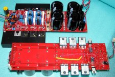
In building my latest version I have come across an anomaly.
I built up the amp board using selected devices.
But I ran out of my "pink" thermal conductors/electrical insulators for the To264 output devices.
I used 5 pink and 1 mica.
Started testing.
The Vre of the mica mounted device is 5mV to 6mV lower than it's partners. All the others are within 1mVre.
Think a bit, check hot, check again when cold (at start up) check again warm and then hot. Same result, the mica mounted Vre is 5mV to 6mV lower.
I must have made a mistake in measuring my devices. I'll swap out the one mica mounted device and replace with another from that set of seven I had measured.
Testing with the replacement has exactly the same result. The Mica mopunted device has a 5mV to 6mV lower Vre. It reads the same as the device that was in there before. The two mica devices could have the "same error". I think not!!!
I have only one explanation.
Could the mica mounted device be running at a different temperature from the 5 partners?
If the mica mounted device is slightly cooler would that Vre difference be as I have described?
While investigating the above problem, I discovered something else that I missed when assembling the Roender PCBs.
If I measure the output offset and the output noise using my DMM when the input has a shorting plug installed I get 0.0mVac and ~2mVdc from all three amplifiers.
If I substitute a 100r dummy phono plug test source for the short I read the same DC but the AC increases to 0.3mVac. This is consistent for the two Roender boards.
With a 1k0 input source I get 1mVac at the output.
I cannot recall the actual results of doing this test on other amplifiers, but this increase in "noise" seems not to be usual.
Has anyone done or found similar, or more importantly found different results?
In building my latest version I have come across an anomaly.
I built up the amp board using selected devices.
But I ran out of my "pink" thermal conductors/electrical insulators for the To264 output devices.
I used 5 pink and 1 mica.
Started testing.
The Vre of the mica mounted device is 5mV to 6mV lower than it's partners. All the others are within 1mVre.
Lower Vbe, not higher?
If higher then that is perfectly normal because mica is a better heat conducting material. The corresponding device mounted on a mica electrical insulator will have a lower temperature than the same device mounted on a textile electrical insulator, hence higher Vbe.
Last edited:
That's the conclusion I came to, but I deliberately did not state which device was colder or hotter.
Yes a cooler device will have a higher Vbe and a lower hFE. These two effects are measurable. Higher base current through the 2r2 and higher Vbe for the mica mounted device.
The two higher voltages subtract from the Vbias/2 that is applied to the output device and this results in a lower bias current. That is what I am measuring.
BUT,
I selected these "pink" insulators from a large range and chose the second best. I decided I could not afford the best ( the ultra low Rth c-s insulators did not exist at that time).
I thought the "pink" was roughly the equivalent to a thin mica insulator from the data supplied by the manufacturer.
I suppose I should not be surprised by exaggeration in manufacturers' data. They are trying to sell their product.
I wonder how the Kerafol would compare.
Finally, I am really surprised how much difference a few C degrees in device temperature has made to the bias current imbalance. 185mA to 245mA thats 32% difference !!!
Last edited:
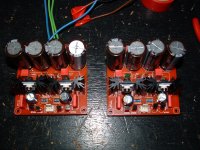
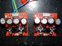
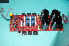
FC100 Pics
Rudi, here are a few pics of my FC100 build. First pic is board with temp heat sink for testing with corrections as per revised build manual and your email. Second pic is of the 2nd PCB undergoing diagnostics...
Unfortunately, I am having problems with both boards so hopefully a common error. At this stage I have only replaced the LED to insure they were inserted with correct polarity as non of them light during testing. The back end and front end PSU's are fine.
All transistors were tested and matched prior to assembly. So far, the only "clue" I have is that when I power up the back end slowly to 35VDC using a variac, the bulb tester lights up dims and goes out but no LED's on front end, nothing heats up and no smoke. Can't adjust the bias. If I power up to 35VDC right away the bulb tester stays on and the 15034 heats up???
If anyone as ideas before I start pulling things apart, I'd love to hear them. Sorry to have to post this in the GB tread!
Jean
Attachments
Jean, I had the same "results" as you have, when I switched on my prototype for the 1.st time.
I advise you to do the 1.st power-on in 2 steps:
1) Remove the fuses of the on-board fuseholders, remove the backend-transformer and only connect the small 34VAC transformer via the bulb-tester.
Then power-on! Do all the LEDs in the frontend shine? If you have an oscilloscope, you can even apply a sine signal to the input and see the output
at the bases of the pre-drivers.
2) Remove the 34VAC-transformer from the bulb-tester, but leave it connected to the frontend!
Insert the fuses into the fuseholders and connect the backend-transformer via the bulb-tester.
Insert jumpers on 2 (!) ThermalTrak - bypass connectors, be sure that the potentiometer is preset to 0 Ohm, and do a short on the input.
Then power-on.
The DMM, which is connected across 2 emitter-resistors (between MP1 and MP2) shoud say: 0mV and the light of the bulb-tester
should shine (a little bit).
Are you able to increase the voltage drop across the 2 emitter resistors?
Best regards - Rudi
- Status
- This old topic is closed. If you want to reopen this topic, contact a moderator using the "Report Post" button.
- Home
- Amplifiers
- Solid State
- Roender's FC-100 prototype and builder's thread