ZDR: your layout looks good - and: you are much faster than I am!
I have two suggestions:
1) I think you are using caps with a diameter of max. 30 mm on the right side of the PCB.
Would you be able to change the caps to the EB35D - Eagle package?
Do we then need 4 capacitors or aren't 2 enough?
2) You talk about a "large MKT" capacitor that you have included. Can we settle on a specific capacitor that I will be able
to offer in this group-buy as well?
What about a Vishay MKT1813 - 1µF / 100V? Its diameter is 8.5mm, its length is 19mm, so the pads shoud have a distance of about 25mm.
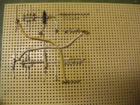
This is my current progress:
http://www.abload.de/img/topviewtyjgj.jpg
I like when everything looks symmetrical.
Comments are welcome.
Best regards - Rudi
I have two suggestions:
1) I think you are using caps with a diameter of max. 30 mm on the right side of the PCB.
Would you be able to change the caps to the EB35D - Eagle package?
Do we then need 4 capacitors or aren't 2 enough?
2) You talk about a "large MKT" capacitor that you have included. Can we settle on a specific capacitor that I will be able
to offer in this group-buy as well?
What about a Vishay MKT1813 - 1µF / 100V? Its diameter is 8.5mm, its length is 19mm, so the pads shoud have a distance of about 25mm.
This is my current progress:

http://www.abload.de/img/topviewtyjgj.jpg
I like when everything looks symmetrical.
Comments are welcome.
Best regards - Rudi
Last edited:
Hi Christoph, Rudi,
If you use the newer On-Semi output transistors, matching is not a problem. They arrive much tighter than matched pairs used to be bought from amplifier manufacturers. No worries there.
I also agree that one or a few people attempting to match sets for a group buy using the older parts would be totally exhausted. A far ir charge for doing this would have everyone making jigs to do it themselves.
To match the smaller (TO-220 and smaller) packages, there is a jig I developed a couple years ago that does the job amazingly well. It's cheap, simple and uses the basic characteristics of transistors to do it's thing. You supply the meter(s). Walt Jung looked it over, and aside from different component values he would rather use gave it his blessing. Personally, I decided to leave it as it was since it worked really very well. Bonus time, you can also use it to match J-Fet transistors. I'll post some of the info next. If anyone wishes to design a PCB for it, I'll be happy to help with some of the design details. Keep in mind that the NPN section was conceived, designed and constructed in one hour as I had an urgent need for it.
-Chris
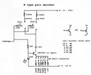
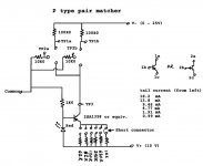
Match'in xistors
Okay, here is some info on it. I may need to add details tomorrow, but I'm tired tonight. Another thing you can do with this jig in addition to simply testing the balance on a pair of transistors is that you can also measure the beta at the test current divided by two if balanced. If you only insert one transistor, you no longer have a compensation for temperature, but at least you are still using a stable test current.
For some of you out there who prefer to match on Vbe only, no sweat, just measure it. However, this jig takes both Vbe and beta into account at the same time.
The most critical thing about this are the resistors. You need close tolerance resistors in matched pairs, but they are cheap. I recently bought some 0.1% resistors for a rebuild. The rest of the circuit is open for modification, nothing sacred here. It was a quick into service deal. In fact, I have worn out the sockets again. It gets a lot of use. You know how close the matches are? Emitter degeneration resistors in a diff pair also need to be matched or they will throw off the match. That is silly close, and it surprised me the first time I ran into this issue.
What would I like to change? The tail current generators.
What would I like to add as a feature? Current mirrored PNP section to NPN current
What would be really cool? Making a setup to match NPN and PNP complimentary pair matching.
One further note. This device will merrily match surface mount components. My adapter is a pain to use. The thing is, this can have adapters to plug in enabling vastly different packages to be assessed. Obviously you can not cut a matched pair package apart, but it would be nice to prove the part was still matched or not. Then there are really cool complimentary pair SM parts, plus packages that have common elements. An adapter board could bridge the NPN and PNP sections and make testing the match on anything.
Here we go...
-Chris
Attachments
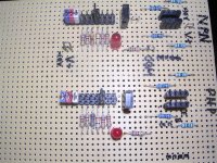
Using the thing
Insert the transistors with the cases touching each other. I made some foam covers that slip over the pair to stabilize the temperature. This creates a common thermal environment for both transistors. They need to be at the same temperature, which only occurs with a match condition. Everything comes together when the transistors are balanced.
Give the parts time to settle down. You can pre-screen transistors by beta groups with the beta function on a DMM. Do your best to keep the temperature constant. Be prepared to see how far apart they really are once you begin balancing them in the jig. Also try to match one beta group up and down - you will find matches.
The sockets have four contacts per part. This way they will accommodate JEDEC, JIS and Pro-Electron pin-outs without having to mangle the leads. These sockets also carry the adapter PCBs, but I'm thinking that separate sockets should be used to prolong the life of the contacts. I used those snap-off terminal sockets you buy in strips. The current set terminals are headers as used on computer motherboards. That's also where the shorting terminals you can see in the pictures came from.
This jig is simply a differential (long tailed) pair with a current source for tail current. Since that is how the transistors you match are most commonly used, you are simply recreating the conditions you will use them in. The tail current is adjustable with the jumpers. The currents will be additive - sort of. It might be more accurate to say the current varies as the setting. That means you can check the balance at different current levels and change those on the fly. Just set the tail current close to what you intend to use in circuit and you will have happy, tight matched pairs.
When installing those freshly minted matched pairs, install them so the encapsulated parts touch. Add a touch of thermal compound between them and use heat shrink tubing to isolate them from the big, bad world. It also holds them together in contact with each other. For real low noise applications, there are brass clips that have a grounding lead that will hold the parts together. Adding silicon around the leads once they are in the PCB and foam (or whatever - plastic cap even) over the parts will eliminate air currents, and also keep the PCB sealed against contamination. If that is important, seal the foil side as well. You can also use copper sheet to form a shield below. That will be electrically quiet. Want to go nuts? Isolate the PCB inside an insulated space and use a regulated heater to maintain a near constant temperature. Drift? What drift?
Where would you find a setup like that I described above? Instrumentation (those real expensive instruments), RF equipment, Frequency standards, Voltage standards, on and on. An extremely quiet phono stage could be done this way if you're into pushing the envelop.
Oh, and don;t forget to install test points for your meter probes on the jig. Might be helpful. I used wire loops the first time (built fast, remember?), but you can buy commercial coloured test points, as well as probe jacks. I'm thinking the probe jack is the way to go, the small pin jacks, not banana sockets!
Edit:
I usually use +/- 10 VDC to run the thing. You can adjust the C-E voltage to whatever is convenient for you, the tail current generator is happy around 10 VDC as well. If you're setting up J-Fets, you might want to keep them in your intended application below about 7 VDC. They make less noise that way.")
-Chris
Insert the transistors with the cases touching each other. I made some foam covers that slip over the pair to stabilize the temperature. This creates a common thermal environment for both transistors. They need to be at the same temperature, which only occurs with a match condition. Everything comes together when the transistors are balanced.
Give the parts time to settle down. You can pre-screen transistors by beta groups with the beta function on a DMM. Do your best to keep the temperature constant. Be prepared to see how far apart they really are once you begin balancing them in the jig. Also try to match one beta group up and down - you will find matches.
The sockets have four contacts per part. This way they will accommodate JEDEC, JIS and Pro-Electron pin-outs without having to mangle the leads. These sockets also carry the adapter PCBs, but I'm thinking that separate sockets should be used to prolong the life of the contacts. I used those snap-off terminal sockets you buy in strips. The current set terminals are headers as used on computer motherboards. That's also where the shorting terminals you can see in the pictures came from.
This jig is simply a differential (long tailed) pair with a current source for tail current. Since that is how the transistors you match are most commonly used, you are simply recreating the conditions you will use them in. The tail current is adjustable with the jumpers. The currents will be additive - sort of. It might be more accurate to say the current varies as the setting. That means you can check the balance at different current levels and change those on the fly. Just set the tail current close to what you intend to use in circuit and you will have happy, tight matched pairs.
When installing those freshly minted matched pairs, install them so the encapsulated parts touch. Add a touch of thermal compound between them and use heat shrink tubing to isolate them from the big, bad world. It also holds them together in contact with each other. For real low noise applications, there are brass clips that have a grounding lead that will hold the parts together. Adding silicon around the leads once they are in the PCB and foam (or whatever - plastic cap even) over the parts will eliminate air currents, and also keep the PCB sealed against contamination. If that is important, seal the foil side as well. You can also use copper sheet to form a shield below. That will be electrically quiet. Want to go nuts? Isolate the PCB inside an insulated space and use a regulated heater to maintain a near constant temperature. Drift? What drift?
Where would you find a setup like that I described above? Instrumentation (those real expensive instruments), RF equipment, Frequency standards, Voltage standards, on and on. An extremely quiet phono stage could be done this way if you're into pushing the envelop.
Oh, and don;t forget to install test points for your meter probes on the jig. Might be helpful. I used wire loops the first time (built fast, remember?), but you can buy commercial coloured test points, as well as probe jacks. I'm thinking the probe jack is the way to go, the small pin jacks, not banana sockets!
Edit:
I usually use +/- 10 VDC to run the thing. You can adjust the C-E voltage to whatever is convenient for you, the tail current generator is happy around 10 VDC as well. If you're setting up J-Fets, you might want to keep them in your intended application below about 7 VDC. They make less noise that way.
-Chris
Last edited:
ZDR: your layout looks good - and: you are much faster than I am!
I have two suggestions:
1) I think you are using caps with a diameter of max. 30 mm on the right side of the PCB.
Would you be able to change the caps to the EB35D - Eagle package?
Do we then need 4 capacitors or aren't 2 enough?
2) You talk about a "large MKT" capacitor that you have included. Can we settle on a specific capacitor that I will be able
to offer in this group-buy as well?
What about a Vishay MKT1813 - 1µF / 100V? Its diameter is 8.5mm, its length is 19mm, so the pads shoud have a distance of about 25mm.
I think we better stick to orginal circuit design, meaning 4 large caps. Experts might chime in on why it could be relevant, I can only guess one - lower total ESR. You can further reduce length by bringing output transistors closer together.
Vishay MKT 1839 is the correct 1uF one I think (unless I ordered wrong one)
Attachments
ZDR,
we do have a low ESR by wiring the capacitors C7 and C8 parallel to the big power cap C17 (C9 and C10 parallel to C13) and placing them
very close to the output-transistors. I do not think that 2 power caps per rail are really needed.
When I will offer this PCB, I would like and offer the "hard-to-get" components as well, like the NJL*-transistors, caps, ...
Call it "a small kit" then.
I do not have access to MKT 1839 / 1µF.
I have access to MKT 1822 and MKT 1813 / 1µF.
I thank you very much for sending me the EAGLE-schematic-files.
I seem to have taken an older version of Mihai's files that did not include the values of the components.
@ANATECH: thank you very much for your explanations how to match transistors.
I hope that it will rain and snow this afternoon.
If so I will have the time to solder a simple matching-circuit.
If not I will go to Hamburg's Christmas market.
Best regards - Rudi_Ratlos
Attachments

I think we better stick to orginal circuit design, meaning 4 large caps. Experts might chime in on why it could be relevant, I can only guess one - lower total ESR. You can further reduce length by bringing output transistors closer together.
Vishay MKT 1839 is the correct 1uF one I think (unless I ordered wrong one)
nice board, I quite like how you've made use of all the wasted space in the front end.
Four caps probably accommodates more users of the board. What are its dimensions?
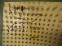
Luke,
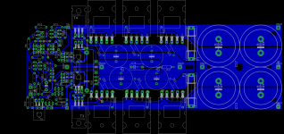
this is the current status of METAL's and my layout:
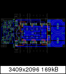
http://www.abload.de/img/lookedthroughwmacr.png
I know that METAL is currently working on the backend (right side of the PCB) to improve the polygons, routing of the tracks, ...
As you can see I changed the power caps to have a diameter of max. 35mm and will use MPC74 emitter resistors.
I also inserted 4 mounting-holes and 6.3mm spades for connecting the power lines.
The frontend (left side) is a copy of ZDR's layout.
Thanks to ZDR I have now a current EAGLE-schematics of the RMI FC-100 with values given.
I will now begin and "optimize" (if possible, ZDR!) the routing of the frontend.
It won't take long anymore until METAL's and my final layout will be published.
The current size of my PCB is 165 x 72 mm.
Best regards - Rudi_Ratlos
Very nice Rudi.
I assume you've decided that one cap is enough?
Other question is do we want connectors for input/output and power? I think they are worth the extra space on the board, its nice to be able to disconnect everything to get the board out and not need a soldering iron. Its also tidy.
I assume you've decided that one cap is enough?
Other question is do we want connectors for input/output and power? I think they are worth the extra space on the board, its nice to be able to disconnect everything to get the board out and not need a soldering iron. Its also tidy.
Rudi, my layout was primarily made for the purpose of single-sided home-brew pcbs, I would not recommend sticking to it for double-sided designs. If you are going for double-sided design, it could be made much better than mine. Also, your output tracks are narow as in my PCB. I had to do it like that since I did not have enough space, but maybe you should use the advantage of DS PSB to make them at least as wide as in original.
Overall, great looking PCB.
Overall, great looking PCB.
Great to have you back Mihai!
We are playing with your pcb layout and trying not to mess up your great design in the process
Rudi has been asking me some questions for which I think you will be in much better position to answer:
1) Why four large caps and not two?
2) Why no AC/DC decoupling caps at the input?
And a question from me:
3) There seems to be lot of serious talk about matching in the main thread, and some really extreme tolerance goals, which totally put me off each time I finally try to finish the amp. I would like to know what matching you did and how for your own working build?
1) Why four large caps and not two?
2) Why no AC/DC decoupling caps at the input?
3) There seems to be lot of serious talk about matching in the main thread, and some really extreme tolerance goals, which totally put me off each time I finally try to finish the amp. I would like to know what matching you did and how for your own working build?
1. Low ESR.
If one do not have room or do not wanna use four general purpose capacitors, I would recommend two low ESR capacitors designated for audio applications.
2. I don't like sound colorations and, if it's possible, I would try to avoid any DC decoupling capacitors. Besides that, any modern audio source have near zero output DC. Moreover, the amplifier have DC 1 voltage amplification. So, what's the point in having an inline input capacitor?
3. Low power BJT or JFET can be effortlessly matched and I would recommend you to do it as close as you can. Anatech describe in the above replay a very good matching method.
It is not hard to match PNP and NPN 0302/0281 parts from ONsemi. I have done that without much effort using a 100mA CCS for Ic and measuring the voltage dropped over an base resistor.
http://www.diyaudio.com/forums/soli...tage-audio-power-amplifier-2.html#post1351876
Hello Mihai,
I appreciate your attention to this thread very much!
My friend METAL and I - after reading a lot of articles of this forum - decided to build your RMI FC-100 amplifier and provide to everybody,
who is interested, the PCBs for it.
Our offer will also include a PCB for the frontend power-supply and "not-easy-to-get-components", such as: output NJL* - transistors,
pre-driver transistors, emitter resistors, small caps: things that will fit in a coated letter.
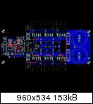
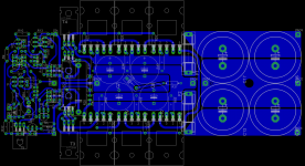
METAL and I have worked on the layout in the last days, and this is the current stage of our design:
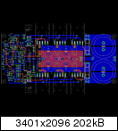
http://www.abload.de/img/topview79zdv.png
The major differences, compared with your design, are:
1) We will only use 2 power caps on the right side, the diameter of which can be 35mm at most
2) We have included a "big EAGLE package" for capacitor C5 that will accept a MKP 1839 (for example) on this position
3) All resistors are mounted horizontally and have the EAGLE package "0207/10"
4) We will use Futaba MPC74 emitter resistors
5) We have included 4 mounting-holes and 6.3mm spades for power- and output-connectors
The frontend is not yet finished and METAL and I still have to do several iterations on it.
We have the feeling that the frontend is too much crowded currently, and maybe we will increase the size on the left side of the PCB by 10mm.
Nevertheless: the above picture will give you an impression, how the layout will finally look like, and I would appreciate very much,
if you can give us your comment on it.
If you like to, I will send you the EAGLE files.
Best regards, many thanks for looking around: Rudi_Ratlos
I appreciate your attention to this thread very much!
My friend METAL and I - after reading a lot of articles of this forum - decided to build your RMI FC-100 amplifier and provide to everybody,
who is interested, the PCBs for it.
Our offer will also include a PCB for the frontend power-supply and "not-easy-to-get-components", such as: output NJL* - transistors,
pre-driver transistors, emitter resistors, small caps: things that will fit in a coated letter.
METAL and I have worked on the layout in the last days, and this is the current stage of our design:

http://www.abload.de/img/topview79zdv.png
The major differences, compared with your design, are:
1) We will only use 2 power caps on the right side, the diameter of which can be 35mm at most
2) We have included a "big EAGLE package" for capacitor C5 that will accept a MKP 1839 (for example) on this position
3) All resistors are mounted horizontally and have the EAGLE package "0207/10"
4) We will use Futaba MPC74 emitter resistors
5) We have included 4 mounting-holes and 6.3mm spades for power- and output-connectors
The frontend is not yet finished and METAL and I still have to do several iterations on it.
We have the feeling that the frontend is too much crowded currently, and maybe we will increase the size on the left side of the PCB by 10mm.
Nevertheless: the above picture will give you an impression, how the layout will finally look like, and I would appreciate very much,
if you can give us your comment on it.
If you like to, I will send you the EAGLE files.
Best regards, many thanks for looking around: Rudi_Ratlos
Hi Rudi
Your effort is laudable! It seams to be a good lucking design but is away from my main PCB design philosophy which can be resumed in few words: Avoid at any cost the parasitic and intrinsic non linear cross layers PCB capacitance, especially if you want to use FR4 substrate.
You should give it a try an see how it works, if it is stable, before offer the PCB to the others.
Best regards,
Mihai
- Status
- This old topic is closed. If you want to reopen this topic, contact a moderator using the "Report Post" button.
- Home
- Amplifiers
- Solid State
- Roender's FC-100 prototype and builder's thread