Gentlemen,
thank you very much for your interest.
In this group-buy my friend METAL and I will offer you PCBs for Mihai Roender's very fabulous RMI FC-100 amplifier.
The design of his amp, technical questions and answers, is covered in this thread:
http://www.diyaudio.com/forums/solid-state/111756-rmi-fc100-single-stage-audio-power-amplifier.html
METAL and I - after building Carlos Mergulhaos' DX Blame ES/ST and Michael Bittner's SYMASYM -
have been thinking a long time:
"Which AMP will be our next DIY - project?
Which AMP can play distinctly and visibly, can offer the whole stage, where the sound is not stuck to a pair of speakers?"
We raked up the AMPs (the schematics) of this forum and finally settled on Mihai's RMI FC-100.
Mihai was friendly enough to publish the EAGLE files for the AMP's - and frontend PSU's - PCBs.
METAL and I will take Mihai's EAGLE files and do some very slight, nearly invisible modifications to his layout, to his way to layout the tracks,
but we will not change anything concerning the schematics and used components of his AMP.
Mihai's RMI FC-100 AMP PCBs have 2 layers: top and bottom.
This is Mihai's original top layer:
http://www.abload.de/img/original_top_layer73k4r.png
This is the top layer of "my" layout - my "EAGLE handwriting":
http://www.abload.de/img/top_layerkdkty.png
The differences may be "peanuts in your eyes".
But I (!) like the tracks being "round and smooth", I do not like small transistors having big, oval pads, I do not like tracks having different width, I do not like ...
I have just begun to rework Mihai's layout: it will take some time, until I am done.
When METAL and I have completed our job, we will offer you:
- the RMI FC-100 AMP PCBs
- the frontend regulated PSU
- if possible I will try and offer you the output NJL0302/NJL0281 transistors
The quality of the PCBs that you can expect, will be like this:
http://www.abload.de/img/to-3_symasym1hkhqvwjto.jpg
The best quality that you can imagine!
METAL has created a formsheet:
https://docs.google.com/spreadsheet/ccc?key=0AjoWwC_y8PtfdG9OZEN0T25aeTlZcHpkcHhxVUQ2clE#gid=0
in which you can sign-in, if you are interested.
I expect the price for a single AMP- or PSU - PCB to be lower than 10€.
Maybe (I hope so) some of the HighEnders of this forum (for example Andrew T., whose recommendations I appreciate very much) or somebody,
who already built this outstanding AMP, or even Mihai himself, will give METAL and me some hints, how to even improve the layout / schematics.
Give METAL and me some time to do our part.
I will come back to you soon.
Best regards - Rudi_Ratlos
thank you very much for your interest.
In this group-buy my friend METAL and I will offer you PCBs for Mihai Roender's very fabulous RMI FC-100 amplifier.
The design of his amp, technical questions and answers, is covered in this thread:
http://www.diyaudio.com/forums/solid-state/111756-rmi-fc100-single-stage-audio-power-amplifier.html
METAL and I - after building Carlos Mergulhaos' DX Blame ES/ST and Michael Bittner's SYMASYM -
have been thinking a long time:
"Which AMP will be our next DIY - project?
Which AMP can play distinctly and visibly, can offer the whole stage, where the sound is not stuck to a pair of speakers?"
We raked up the AMPs (the schematics) of this forum and finally settled on Mihai's RMI FC-100.
Mihai was friendly enough to publish the EAGLE files for the AMP's - and frontend PSU's - PCBs.
METAL and I will take Mihai's EAGLE files and do some very slight, nearly invisible modifications to his layout, to his way to layout the tracks,
but we will not change anything concerning the schematics and used components of his AMP.
Mihai's RMI FC-100 AMP PCBs have 2 layers: top and bottom.
This is Mihai's original top layer:

http://www.abload.de/img/original_top_layer73k4r.png
This is the top layer of "my" layout - my "EAGLE handwriting":

http://www.abload.de/img/top_layerkdkty.png
The differences may be "peanuts in your eyes".
But I (!) like the tracks being "round and smooth", I do not like small transistors having big, oval pads, I do not like tracks having different width, I do not like ...
I have just begun to rework Mihai's layout: it will take some time, until I am done.
When METAL and I have completed our job, we will offer you:
- the RMI FC-100 AMP PCBs
- the frontend regulated PSU
- if possible I will try and offer you the output NJL0302/NJL0281 transistors
The quality of the PCBs that you can expect, will be like this:

http://www.abload.de/img/to-3_symasym1hkhqvwjto.jpg
The best quality that you can imagine!
METAL has created a formsheet:
https://docs.google.com/spreadsheet/ccc?key=0AjoWwC_y8PtfdG9OZEN0T25aeTlZcHpkcHhxVUQ2clE#gid=0
in which you can sign-in, if you are interested.
I expect the price for a single AMP- or PSU - PCB to be lower than 10€.
Maybe (I hope so) some of the HighEnders of this forum (for example Andrew T., whose recommendations I appreciate very much) or somebody,
who already built this outstanding AMP, or even Mihai himself, will give METAL and me some hints, how to even improve the layout / schematics.
Give METAL and me some time to do our part.
I will come back to you soon.
Best regards - Rudi_Ratlos
Gentlemen,
output NPN- and PNP- transistors cannot be matched!
The NPN-NJL0281D - and PNP-NJL0302D - transistors themselves are usually matched by the fabrication process within 10%!
What is more important than to match the output-transistors is to match the transistors of the input differential amplifier: the 2SK170.
There are 2 types of 2SK170: 2SK170BL and 2SK170GR.
Which type does Mihai recommend?
What about matching the BC550C and BC560C? I will read through Mihai's thread again!
Is anybody of you able to provide some matched pairs of 2SK170, BC550C and BC560C?
Best regards - Rudi
Outputtransistors
Rudi, Mihai strongly recommended matching of the outputtransistors. Some time ago I bought some of them and saw big differences......
Matching 550 etc is not a big deal, needs just a DMM and a few of these cheapies.
SK170: You can buy them matched for not too much money from a nice guy which is a diyaudio member (forgot his diyname) and has an ebay shop for such things. I've bought some parts from him and was always happy with them.
Regards Ernst
Hi Rudi,
I agree with Ernst also, but I'll add more.
Try to match the complementary transistors, like drivers. Match any current mirror transistors and of course the diff pair.
If you use the On Semi transistors, their parts match more closely from both each other and NPN to PNP as well. The very best I ever saw were the MJW0281A and MJW0302A. Each measured very close to a beta of 100, both NPN and PNP. Outstanding. Using matched outputs can reduce THD before distortion by a factor of 10 (yes, 10X) before feedback is applied. This is noted in some On Semi data sheets. Another happy fact is that your required bias current also becomes much lower for minimum distortion measurements, even at 10 KHz and higher.
Now to measure transistor beta, you need a jig, not just a meter. Beta is also temperature sensitive as well as current sensitive. So unless you can control the temperature and test current, you need to build something that will run a bunch of transistors up to a temperature and measure them all at the same current. I do this sometimes when experimenting and to confirm measurements from other methods.
-Chris
I drove to Hamburg this morning, bought a couple of NJL0302 and NJL0281 transistors and measured the hFe of the transistors
with my old Voltcraft DMM.

http://www.abload.de/img/joe006xfomz.jpg
Here is the result:
http://www.abload.de/img/joe008yvrm6.jpg
I am sorry to tell you that I could not measure the hFe of the NJL0281 transistors, since the NPN - hFe - section of my DMM did not work properly.
The result of the PNP's hFe measurement is quite promising.
All values are within 5% deviation of a "standard hFe" of 95.
In my eyes selecting proper pairs of output transistors will not be a NOGO for this DIY project.
Best regards - Rudi_Ratlos
with my old Voltcraft DMM.

http://www.abload.de/img/joe006xfomz.jpg
Here is the result:

http://www.abload.de/img/joe008yvrm6.jpg
I am sorry to tell you that I could not measure the hFe of the NJL0281 transistors, since the NPN - hFe - section of my DMM did not work properly.
The result of the PNP's hFe measurement is quite promising.
All values are within 5% deviation of a "standard hFe" of 95.
In my eyes selecting proper pairs of output transistors will not be a NOGO for this DIY project.
Best regards - Rudi_Ratlos
METAL is right.
I will not offer matched pairs of output-transistors in this group-buy.
Matching - hFe and Vbe - of transistors is very time-consuming!
But I can - if you agree - order several hundreds of them from Mouser or DIGIKEY or ..., from any distributor, who has them on stock,
and ship them together with your PCB order.
Best regards - Rudi_Ratlos
METAL is right.
I will not offer matched pairs of output-transistors in this group-buy.
Matching - hFe and Vbe - of transistors is very time-consuming!
But I can - if you agree - order several hundreds of them from Mouser or DIGIKEY or ..., from any distributor, who has them on stock,
and ship them together with your PCB order.
Best regards - Rudi_Ratlos
How tight have these NJL output transistors to be matched for the Roender RMI FC-100 amp?
Anyone out there with experience with this parts who can advise a ballpark number how many would be needed to get matched sets for let`s say 10 amps (I reckon building more amps need comparatively "less more" devices than building only one pair)?
A question regarding the front-end power-supply PCB:
I believe the V-Reg circuit on the front-end Power-Suppy PCB would be beefy enough to feed several amp front-end circuits (boards).
Is this correct?
If so and to do so, will there be solder-pads for multiple output connectors on the front-end PS-PCB?
links do work fine for meRudi,
I can't expand your pics/links.
You persist in using a remote server.
Hello Christoph,
I did some rough hFE matching yesterday, and the results looked promising.
In one of his posts, Mihai writes that the output transistors should be matched for both hFE and VBe to stay in Class A operation
as long as possible without overdriving (correct word?) the bias.
Maybe I will solder a small circuit this weekend and measure the VBe of my transistors.
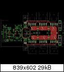
METAL and I exchanged our views on Mihai's PCB yesterday.
Find enclosed his current layout.
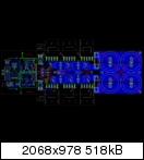
http://www.abload.de/img/lookedthroughhfvn7.png
(Andrew: I will try and use the forum's attach function in future!)
There are several issues METAL and I found regarding Mihai's layout:
1) Either the reworked layout will include a "mature" PSU on the right side (allowing for caps with 35mm diameter for example,
integrating a "C - L/R - C - filter", why not the rectifier diodes as well?) or it will be completely removed from the PCB
2) The reworked PCB will include EMI protection (sorry for the typo in the image)
3) The current layout does not give sufficient space to the Zobel capacitor
4) There are 4 capacitors near the pre-drivers that do not fit in this position.
In some of Mihai's pictures of his PCB I see that he is using big µF WIMA caps on this position, but the EAGLE .brd-file gives only room
for 10 x 3mm MKS3 caps with a grid of 7.62mm
(By the way: can anybody send me the current schematics with values? I found a picture of the schematics in Mihai's original thread,
but this picture does not correspond to the EAGLE schematics file!)
5) The frondend (on the left) shows a lot of unused space. The PCB can therefore made be smaller.
6) I myself do not like resistors being mounted vertically! I will - for example - try and use MPC74 - typ emitter resistors!
Mihai's PCB layout is quite good, for sure, but it can be improved!
METAL and I will now check how easily these modifications can be made and if they will introduce any stability issues.
I am a "straight-forward, passionsless" DIYer - and: I am not a millionaire.
I like to do a layout, solder an AMP and get it running.
I will not buy 25 NJL transistors of each NPN- and PNP type, just to get 6 hFE- and VBe - matched pairs.
METAL and I will do our best.
Best regards - Rudi_Ratlos
I did some rough hFE matching yesterday, and the results looked promising.
In one of his posts, Mihai writes that the output transistors should be matched for both hFE and VBe to stay in Class A operation
as long as possible without overdriving (correct word?) the bias.
Maybe I will solder a small circuit this weekend and measure the VBe of my transistors.
METAL and I exchanged our views on Mihai's PCB yesterday.
Find enclosed his current layout.

http://www.abload.de/img/lookedthroughhfvn7.png
(Andrew: I will try and use the forum's attach function in future!)
There are several issues METAL and I found regarding Mihai's layout:
1) Either the reworked layout will include a "mature" PSU on the right side (allowing for caps with 35mm diameter for example,
integrating a "C - L/R - C - filter", why not the rectifier diodes as well?) or it will be completely removed from the PCB
2) The reworked PCB will include EMI protection (sorry for the typo in the image)
3) The current layout does not give sufficient space to the Zobel capacitor
4) There are 4 capacitors near the pre-drivers that do not fit in this position.
In some of Mihai's pictures of his PCB I see that he is using big µF WIMA caps on this position, but the EAGLE .brd-file gives only room
for 10 x 3mm MKS3 caps with a grid of 7.62mm
(By the way: can anybody send me the current schematics with values? I found a picture of the schematics in Mihai's original thread,
but this picture does not correspond to the EAGLE schematics file!)
5) The frondend (on the left) shows a lot of unused space. The PCB can therefore made be smaller.
6) I myself do not like resistors being mounted vertically! I will - for example - try and use MPC74 - typ emitter resistors!
Mihai's PCB layout is quite good, for sure, but it can be improved!
METAL and I will now check how easily these modifications can be made and if they will introduce any stability issues.
I am a "straight-forward, passionsless" DIYer - and: I am not a millionaire.
I like to do a layout, solder an AMP and get it running.
I will not buy 25 NJL transistors of each NPN- and PNP type, just to get 6 hFE- and VBe - matched pairs.
METAL and I will do our best.
Best regards - Rudi_Ratlos
1) or it will be completely removed from the PCB
5) The frontend (on the left) shows a lot of unused space. The PCB can therefore made be smaller.
My 0.02 EUR: The presence of certain amount of large C near the power drivers helps to cope with instantaneous peak signal loads better.
Existing layout allows to use a heat sink with large flat back surface and the power drivers parallel to PCB, PCB itself parallel to heat sink. I wanted to build two mono blocks with power transistors perpendicular to PCB squeezed between two smaller heat sinks in a construction, resembling medium size UPS (dimensions, not functionality
") ). However I will not obstruct the initiators of this GB in any way ;-)
). However I will not obstruct the initiators of this GB in any way ;-)2SK170 matched
It would be nice if the layout would allow to use a LSK389
Linear Integrated Systems - Press Release
instead of two matched 2SK170s. The LSK389 is available
and factory matched. (And you can be sure not to buy
counterfeits.)
It would be nice if the layout would allow to use a LSK389
Linear Integrated Systems - Press Release
instead of two matched 2SK170s. The LSK389 is available
and factory matched. (And you can be sure not to buy
counterfeits.)
Maybe (I hope so) some of the HighEnders of this forum (for example Andrew T., whose recommendations I appreciate very much) or somebody,
who already built this outstanding AMP, or even Mihai himself, will give METAL and me some hints, how to even improve the layout
Two suggestions:
Enlarge the access holes for mounting Q9,13,15 (original schema, 2SA/SC parts). Make them large enough to pass the mounting screw and grommet. Trying to place the screw and grommet/washer from underneath the board is difficult.
Size the front end supply and align the mounting holes so that it can be stacked over the front end with stand offs. Would even be nice to have the power connection between front end and front end supply done with aligned connector.
Sheldon
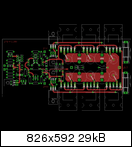
Gentlemen,
I took an hour or so to rework the PSU on the right side of the PCB (the PSU will now accommodate power-caps with a diameter of 35mm)
and the positive output rail.
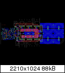
http://www.abload.de/img/top_layerkj3xk.png
Compare it to the negative power rail output (which is unchanged).
Do you see the differences, how "easy-going and smooth" everything can be, if you just spend some time
and draw an EAGLE-package for the famous FUTABA MPC74 emitter-resistors, redraw several EAGLE polygons, ...?
It causes me nightmares to see some resistors being mounted vertically, some of them being mounted horizontally,
some of them being mounted with an angle of 315 (or so) degrees, ...
In my eyes: everything shall be done straight-forward.
But - also in my eyes - the layout contributes only a small amount of the success to this project.
What does really concern me is: how important is HFe- and VBe - matching of the NJL-transistors for this project?
I will now solder a small circuit, match my NPN NJL* transistors and will give you the results tomorrow.
Best regards - Rudi_Ratlos
Hi Rudi,
if you look at Mihai's board,
http://www.diyaudio.com/forums/soli...-stage-audio-power-amplifier.html#post1348705
it appears that the weight of the board is suspended by the transistors mounted on the heatsink. I imagine long term this may cause reliability problems. Finding room for 6 mounting holes on each board may be beneficial.
The PCB already has plenty of empty spaces to drill mounting holes. Don't make it any bigger.
In my opinion one should be striving to make it smaller, particularly much shorter.
The transistors mounted on the flat back heatsink provide 42 legs for mounting the PCB to the sink.
I cannot see where reliability comes into it. Have you tried moving the PCB relative to the sink?
In my opinion one should be striving to make it smaller, particularly much shorter.
The transistors mounted on the flat back heatsink provide 42 legs for mounting the PCB to the sink.
I cannot see where reliability comes into it. Have you tried moving the PCB relative to the sink?
- Status
- This old topic is closed. If you want to reopen this topic, contact a moderator using the "Report Post" button.
- Home
- Amplifiers
- Solid State
- Roender's FC-100 prototype and builder's thread