Mihai,
I did some research on "parasitic and intrinsic non linear cross layers PCB capacitance" in the INTERNET and came across some interesting articles.
For example:
Parallel Plate Capacitor Capacitance Calculator
allows me to calculate the cross-layer capacitance that I introduced with the layout presented it post #38.
Provided that my GND-plane has a size of about 15 square centimeters, the capacitance that I have introduced by my layout is about 31.2 pf.
What is interesting as well is that the articles tell about effects introduced by any cross-layer capacitances.
It seems that you are misregarding your own recommendations, since your layout shows a cross-layer capacitance between
the output-track and the +/- backend power tracks with approximately the same value.
Allthough the value of about 30pF is very small, it means to have a capacitor in parallel to the speaker, "which may be risky".
METAL and I re-designed the tracks on the backend and will avoid any cross-layer capacitances in the new layout.
I have 2 questions to you:
1) The position of the GND-leg of the ZOBEL's cap in the middle of the frontend ("the small signal's) GND - plane:
Is it wise to put it there? Shouldn't I better define a third, isolated GND-PAD and run a wire from there to the STAR-Ground?
2) My second questions is related to the takeoff-point of the NFB.
Dr. Self recommends a point "that is in some distance from where the 2 half-waves come together".
In your RMI FC-100 thread somebody wrote that he has run a small shielded cable from the NFB takeoff to resistor R18.
Do you approve this idea?
@LUKE: your 12.000µF ELNA capacitor is very applicable! Do not forget that you have capacitors C7 and C8 in parallel to it,
summing up to a total capacitance of about 16.000µF per power rail. This should be enough!
I am looking to your answer, Mihai.
Best regards - Rudi_Ratlos
Last edited:
Hi Rudi,
There are always some trade-offs in any good PCB design and you should know that there is no free meal")
If I had to choose between dirty ground plane and dirty power supply lines, which by the way are already affected by half waves output currents (when the amp is passing from A to B classe), I would always choose a clean reference ground. Hence I had preferred to have thick power lines capacitively coupled with the output plane.
Now, regarding your questions:
1. The zobel's network ground point is connected exactly where it should be, at the returning speaker's ground point, and, in fact, that point is the star ground.
2. The NFB take of point is designed in strictly accordance with Dr. Self recommendations. I am not convinced that a shielded cable will improve amplifier's performance or stability.
I wanna make myself clear again. I'm glad that you wanna redesign a tested PCB in order to accommodate various components but you have to test your RMI-FC100 amp based on newly designed PCB before offer it to others.
Best Regards,
Mihai
There are always some trade-offs in any good PCB design and you should know that there is no free meal
If I had to choose between dirty ground plane and dirty power supply lines, which by the way are already affected by half waves output currents (when the amp is passing from A to B classe), I would always choose a clean reference ground. Hence I had preferred to have thick power lines capacitively coupled with the output plane.
Now, regarding your questions:
1. The zobel's network ground point is connected exactly where it should be, at the returning speaker's ground point, and, in fact, that point is the star ground.
2. The NFB take of point is designed in strictly accordance with Dr. Self recommendations. I am not convinced that a shielded cable will improve amplifier's performance or stability.
I wanna make myself clear again. I'm glad that you wanna redesign a tested PCB in order to accommodate various components but you have to test your RMI-FC100 amp based on newly designed PCB before offer it to others.
Best Regards,
Mihai
Last edited:
My friend METAL and I did some work on revision 2 of the layout for Mihai's RMI FC-100 yesterday and - with some pride -
will show you the current stage:
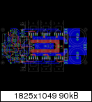
http://www.abload.de/img/topviewrcys0.png
We tried to avoid any parasitic capacitance on the backend and did a tight but smooth layout of the frontend.
Moreover I inserted a decoupling capacitor at the input for those of you DIYers, who connect DIYed attenuators, source selectors, pre-AMPs, ...
to this AMP. The use of this capacitor can be deactivated - for the sake of sound - buy a simple jumper.
We will now check the schematics once more, compare it to the layout (this will be done automatically by EAGLE), do some additional cosmetics,
prepare the silkscreen, ...
The size of the PCB is: 173 x 73 mm.
Best regards - Rudi_Ratlos
I see, what you mean, Andrew:
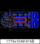
http://www.abload.de/img/topviewlgbqv.png
If you do not like to use the PSU on the right side, you may cut the PCB at the indicated line.
I can ask and insert a "predetermined breaking point " there.
Question: Shall I put the rectifier-diodes on the right side of the PCB as well?
Best regards - Rudi_Ratlos
P.S.: Andrew: still 40 days to go.
I'd modify the traces around the mounting hole for the 2SC3423 transistors that are mounted under the board, so that the access hole can be sized generously. The 2SA1360 is good. Speaking from experience, you want plenty of room to insert the mounting screws and washers from the top of the board.
Sheldon
Sheldon
I would say "no" to putting rectifiers on board.
I would suggest adding a place to put in an optional rail-to-rail capacitor.
Bob Cordell has advocated using at least a 500uf cap for this purpose.
This would be especially useful if the main PS caps were taken off board.
A typical radial snap in cap of 560uf/100v rating would have a 10mm lead spacing, and be 22-25mm in diameter.
ECO-S2AP681BA Panasonic Electronic Components Aluminum Electrolytic Capacitors - Snap In
While there doesn't appear to be any room presently for a radial cap, even if shorter fuses were used, perhaps a plurality of smaller value axial caps could be mounted under the board and connected rail-to-rail around the area of the emitter resistors. This might not be practical, either, due to the diameter of the axial caps causing to great a spacing between the board and heat sink.
Whether or not this is provided, space could easily be provided for an axial cap along and to the left of the break line, especially if the break line was moved slightly to the right to accommodate the diameter of the axial cap. The star ground could then be shifted between the ends of the fuses. This would be really helpful to those who take the main caps off board, providing a shorter path for half-wave currents that would normally circulate back to the main caps off board.
Regarding the fuses, I would recommend providing options for different length fuses. Further, vias could be added for soldering in a fuse like this:
http://www.cdiweb.com/datasheets/cet/OC-2116.pdf
Last edited:
@Sheldon: please have a look at this image:
http://www.diyaudio.com/forums/solid-state/111756-rmi-fc100-single-stage-audio-power-amplifier.html Post #2
This is, how it has to be done.
Best regards - Rudi_Ratlos
http://www.diyaudio.com/forums/solid-state/111756-rmi-fc100-single-stage-audio-power-amplifier.html Post #2
This is, how it has to be done.
Best regards - Rudi_Ratlos
@Sheldon: please have a look at this image:
http://www.diyaudio.com/forums/solid-state/111756-rmi-fc100-single-stage-audio-power-amplifier.html Post #2
This is, how it has to be done.
I've built two of the amps, and I'm familiar with the entire thread. Yes, to avoid strain on the leads it's best to mount the transistors to the heat sink, before placing the board and soldering. You don't even need access holes if you never intend to remove the board from the heat sink after assembly. But if you do want to remove it, replacing it will be easier if you make the access holes generous. I've offered the suggestion based on my personal experience with this amp. But your board, your choice. I have no dog in the hunt.
Sheldon
Pooge, this is what I am thinking about:
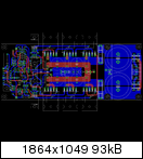
http://www.abload.de/img/topview_psugelwy.png
The size of the PCB has increased by 10 mm.
If somebody wants to use the on-board PSU: he has it and only needs a transformer to get a channel running.
If he does not like the on-board PSU, because he has a better on, he can cut the PCB at the indicated line.
To insert alternative types of fuses, ...: that is very easy to do.
Best regards - Rudi_Ratlos
Pooge, this is what I am thinking about:
http://www.abload.de/img/topview_psugelwy.png
The size of the PCB has increased by 10 mm.
If somebody wants to use the on-board PSU: he has it and only needs a transformer to get a channel running.
If he does not like the on-board PSU, because he has a better on, he can cut the PCB at the indicated line.
To insert alternative types of fuses, ...: that is very easy to do.
Best regards - Rudi_Ratlos
Yes, it is easy to provide vias for different fuse holder lengths. Although different lengths can be obtained by everyone, Europe and USA tend to favor different lengths, and good ones of each type may not be readily available at the same parts suppliers used to buy other parts. So choices are good. Also, a choice of the soldered in fuses without a holder would be nice.
Regarding your latest board, if you break away the rectifier arrangement, the caps come with it. Not a good choice. Some, like me, would prefer a dual bridge, anyway, and have at least some main caps on board. These rectifiers should preferably have heat sinks, also.
I too prefer to use two rectifiers, this is one of the reasons I avoided adding the rectifiers on the PCB, Rudi like to use one rectifier. Sometimes I think about providing a small PCB that only holds the rectifiers, but always turns out to be a silly idea and I forget about it.
Last edited:
Here is a picture, how Mihai himself did it.
http://www.diyaudio.com/forums/solid-state/111756-rmi-fc100-single-stage-audio-power-amplifier.html Post #5
METAL: I read so many articles on using a single or 2 rectifiers, but I neither found a stringent PRO nor a CONS for either of the 2 solutions.
Best regards - Rudi_Ratlos
http://www.diyaudio.com/forums/solid-state/111756-rmi-fc100-single-stage-audio-power-amplifier.html Post #5
METAL: I read so many articles on using a single or 2 rectifiers, but I neither found a stringent PRO nor a CONS for either of the 2 solutions.
Best regards - Rudi_Ratlos
METAL: I read so many articles on using a single or 2 rectifiers, but I neither found a stringent PRO nor a CONS for either of the 2 solutions.
Best regards - Rudi_Ratlos
See post #38 here:
http://www.diyaudio.com/forums/chip-amps/12162-2-rectifier-bridges-why.html#post143874
And post #148 here:
http://www.diyaudio.com/forums/soli...l-interview-power-supplies-4.html#post1067745
The bottom line is that the ground line is not contaminated with charging currents, and the transformers can be quieter.
That being said, it would be preferrable to have separate ground lines for each capacitor input to the board, and that they not be connected together on the board until the star ground. This would allow those who prefer dual bridges to connect them that way, and it would NOT inhibite single bridge users to do it their way. Further, if each rail line input had a "ground" return input placed close to it on the right side of the board, the rail and return lines for each polarity could be twisted together right up to the board. Single bridge users could still run a ground line from each cap back to the transformer center tap.
Last edited:
Pooge, I read somewhere that putting rail to rail caps across opamps slowed them down and should be avoided, wouldn't this apply to power amps?
I have no idea why this would be true. I have never read such a thing, so I can't comment on it. However, one would not have to use the option if it is available.
With onboard caps, a rail-to-rail cap may not be as useful as when caps are off board. The idea is to minimize the size of charging current loops that can couple half wave charging currents into the circuitry. A rail-to-rail cap on board can minimize the size of this loop carrying half wave currents compared to lines going off board to off-board caps. This is why I suggested at least a provision for an axial cap to the left of the break line in case the cap provision was broken off.
If fact, it seems it would not hurt to have the rail and return traces for each cap placed on opposite sides of the board. The capacitance between these traces should not hurt, but help. This keeps the traces very close together to reduce radiation due to charging currents, and again allows connectors to be very close together for twisted pair lines up to the board. Place the star ground between the fuse ends, and run the ground return path from the star ground under each fuse back to each cap. This keeps each of these loops as small as possible.
Last edited:
- Status
- This old topic is closed. If you want to reopen this topic, contact a moderator using the "Report Post" button.
- Home
- Amplifiers
- Solid State
- Roender's FC-100 prototype and builder's thread