You definitely need a scope to see crossover distortion, especially low level distortion.
You can hear bad or medium crossover distorion as a harshness in the sound at low level.
Push pull can give excellent results. I have designed a few mosfet amps and all of them had no crossover distortion when the bias was tweaked correctly. In fact I was gobsmacked at sometimes how little bias was needed to get rid of crossover distortion.
I have used irfp240/9240 with good results.
Jcx, you gotta stay realistic..... But, for linear small (current) signal operation the Vgs/Ids curve at that small scale is still linear. FYI I've experimented a lot with HEXfets in control loops and have quite a good understanding of how they behave for real.
Not-realistic. The low current operating area is highly non-linear because Gm is quite non-linear in this region. Vertical FETs have an exponential transfer so they become more 'linear' (relatively) at higher currents. Because generally an exponential function is far from linear, it is assumed that these devices, like all active devices, create distortion related to their transfer. Vgs vs Id changes more for % change in Id at low current operating region because of the inherent transconductance droop that exists with Mosfets for vertical or lateral structures at low conductance. The big advantage of laterals is the zero temp co is at the bias level for class AB, as opposed to the zero temp co bias for verticals being several amps depending on Gm. Also lateral FETs have a square law transfer as opposed to exponential. Big difference in distortion components.
You definitely need a scope to see crossover distortion, especially low level distortion.
You can hear bad or medium crossover distortion as a harshness in the sound at low level.
Push pull can give excellent results. I have designed a few mosfet amps and all of them had no crossover distortion when the bias was tweaked correctly. In fact I was gobsmacked at sometimes how little bias was needed to get rid of crossover distortion.
I have used irfp240/9240 with good results.
At low currents, below 200-300mA, I wonder what distortion components is created by the Gm droop and traveling through the feedback loop, and what harmonics of those components is generated by the loop. Hmmm.

At low currents, below 200-300mA, I wonder what distortion components is created by the Gm droop and traveling through the feedback loop, and what harmonics of those components is generated by the loop. Hmmm.
I have scoped the output of the amplifier and the sine wave looks really good. The amps sound great which is the proof of the pudding.
I have got as low as 10mA bias current and no crossover distortion.
It would be interesting to get a distortion analyser on it too see what is really being put out tho.
Not-realistic. The low current operating area is highly non-linear because Gm is quite non-linear in this region. Vertical FETs have an exponential transfer so they become more 'linear' (relatively) at higher currents. Because generally an exponential function is far from linear, it is assumed that these devices, like all active devices, create distortion related to their transfer. Vgs vs Id changes more for % change in Id at low current operating region because of the inherent transconductance droop that exists with Mosfets for vertical or lateral structures at low conductance. The big advantage of laterals is the zero temp co is at the bias level for class AB, as opposed to the zero temp co bias for verticals being several amps depending on Gm. Also lateral FETs have a square law transfer as opposed to exponential. Big difference in distortion components.
At low currents, below 200-300mA, I wonder what distortion components is created by the Gm droop and traveling through the feedback loop, and what harmonics of those components is generated by the loop. Hmmm.
Hi CBS240. Yes, I know that the transfer curve is not a straight line, no matter what scale. But as you say, higher up the slope it is more lineair than at low currents. But you also have to take into account current swing, your active operating range. Used as output devices you indeed going to need a sufficient current, after all, used as output transistor you're operating on a much bigger scale, 0 - couple amps per transistor. On the contrary, when used as FET output stage driver, quiescent current is fixed with very small fluctuations in current due to the loading by its output stage. That, is small scale. And what's lineair at a large scale is just as lineair at a small scale with a small load. The same goes for cascode operation; under normal conditions there's hardly any current swing in the VAS rail, the active current fluctuation range is very small. It's not a good idea to just blindly pick parts but also regard the circumstances it's used in. In my amp for example, the VAS current is around 35mA with fluctuations in the several 10s of uA.
Just to be clear, I'm not advocating low bias currents for output FETs, that's probably where some misunderstanding is coming from
")
Last edited:
At low currents, below 200-300mA, I wonder what distortion components is created by the Gm droop and traveling through the feedback loop, and what harmonics of those components is generated by the loop. Hmmm.
May he (nigel) mean if it underbiased. Hi,CBS. Do you have another EC or still using your old one?
Not-realistic. The low current operating area is highly non-linear because Gm is quite non-linear in this region. Vertical FETs have an exponential transfer so they become more 'linear' (relatively) at higher currents. Because generally an exponential function is far from linear, it is assumed that these devices, like all active devices, create distortion related to their transfer. Vgs vs Id changes more for % change in Id at low current operating region because of the inherent transconductance droop that exists with Mosfets for vertical or lateral structures at low conductance. The big advantage of laterals is the zero temp co is at the bias level for class AB, as opposed to the zero temp co bias for verticals being several amps depending on Gm. Also lateral FETs have a square law transfer as opposed to exponential. Big difference in distortion components.
At low currents, below 200-300mA, I wonder what distortion components is created by the Gm droop and traveling through the feedback loop, and what harmonics of those components is generated by the loop. Hmmm.
It's worth noting that verticals and laterals both obey the same model, just with different numbers. Specifically, both have a sub-threshold region (weak inversion) where their Id vs Vgs obeys an exponential law, just like BJTs do (but again, with different numbers. Above the sub-threshold region, both laterals and verticals obey the square law. At still higher currents the characteristic transitions into another region where behavior is more dominated by effective source resistance. The SPICE EKV model, discussed in my book, is fairly accurate in modeling these behaviors.
Cheers,
Bob
Hi Bob,
Everyone said that they are different.
I also have found that they switched easily than laterals, more in higher Vds. Not happened in SPICE level 1 simulation but happened in level 3. higher Vds effect only happened in real and not happened in level3 simulation. Dont no why.
What is EKV SPICE model, I am currently using SPICE level3 MOSFETS model.
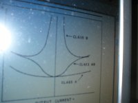
Nelson in his A40 article touches on another effect that hapens in the crossover
region. The output impedience where it is verry high in the crossover region of a class B amp and is lower and more stable in a class A output stage. Here Is a crude
picture from the pdf of the article. I didn't know how to export a picture so I just
took a picture. I wonder if the difference in output impedience effects speaker damping. Taking to an extreme supose an amp had an output impedience of .1 ohm
at 10 mw but had an output impedience of 10 ohms at 10 W couldn't that realy mess
up the frequency responce.
Attachments
Hi Bob,
Everyone said that they are different.
I also have found that they switched easily than laterals, more in higher Vds. Not happened in SPICE level 1 simulation but happened in level 3. higher Vds effect only happened in real and not happened in level3 simulation. Dont no why.
What is EKV SPICE model, I am currently using SPICE level3 MOSFETS model.
Verticals and laterals have very different construction, but pretty much the same mode.ling issues. Neither one is properly modeled by level1 or level 3 SPICE. The EKV model (as I sit here in the airport I don't recall what the EKV stands for, but I think it is three guys) correctly models sub-threshold conduction, which all types of MOSFETs exhibit. Because the numbers that are used in the models of laterals and verticals are different, their real-world behavior is quite different.
I discuss the EKV model in my book (Designing Audio Power Amplifiers) and show how to create one's own models with one's own laboratory measurements.
Sometime soon I hope to be able to post EKV models for laterals and verticals on my website at CordellAudio.com - Home. Stay tuned.
Cheers,
Bob
Nelson in his A40 article touches on another effect that hapens in the crossover
region. The output impedience where it is verry high in the crossover region of a class B amp and is lower and more stable in a class A output stage. Here Is a crude
picture from the pdf of the article. I didn't know how to export a picture so I just
took a picture. I wonder if the difference in output impedience effects speaker damping. Taking to an extreme supose an amp had an output impedience of .1 ohm
at 10 mw but had an output impedience of 10 ohms at 10 W couldn't that realy mess
up the frequency responce.
Hi Woody,
You will find extensive discussions on crossover distortion in my book, both for MOSFETs and Bipolars when used in push-pull output stages. An under-biased class AB BJT output stage has its output impedance rise as the output current goes through the crossover region, and its incremental gain will decrease, causing distortion. An over-biased class AB BJT output stage will exhibit a lower output impedance in the crossover region, leading to a phenomenon sometimes called gm doubling. MOSFET class AB output stages suffer from transconductance droop, originally described in my AES paper on a MOSFET power amplifier with error correction about 30 years ago. With transconductance droop, the output impedance increases as the output current goes through the crossover region, and the output stage incremental gain goes down, causing distortion.
Cheers,
Bob
- Status
- This old topic is closed. If you want to reopen this topic, contact a moderator using the "Report Post" button.
- Home
- Amplifiers
- Solid State
- Crossover distortion in push-pull