I've been revisiting at some "simple" amp designs, notably the JLH 10W and the Pass Z5. Both appeal to me in different ways and I'm a sucker for alternative topologies...
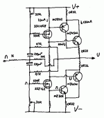
I was toying with this circuit late last night so it hasn't been thought through entirely. I'm not able to attempt a simulation at present. Some of the component values are straight out of the Z5 (apologies to Nelson).
The idea was to do something substantially "different" and combine CC and CE output devices, in this case in a class AB o/p stage. What does the forum think? Nelson? Anybody willing to have a go at simulating? I'm a bit worried those BJT's are going to oscillate. BTW the parts designations merely reflect what I have lying around at the moment.
All constructive (and destructive) criticism welcomed...
Attachments
Better add some protection diodes to those MOSFETs lest you get yourself ripped a new one for posting such an irresponsible schematic. ")
Looks like you've achieved your design goals, but it doesn't exactly scream "simple" with half a dozen or so more parts than the Zv5.
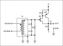
If you want a CC/CE combination and simple, how 'bout something like this?
Looks like you've achieved your design goals, but it doesn't exactly scream "simple" with half a dozen or so more parts than the Zv5.
If you want a CC/CE combination and simple, how 'bout something like this?
Attachments

jam said:I knew you would find a way to stick a transformer in there!
Transformer? Oh crap! That was supposed to be an opamp!
se
jam said:Had to pull it ..........moderators seem to be a bit edgy today.
No joke? What on earth was wrong with it!?
se

jam said:Well what the heck. I have never been to the sinbin.
My response was...
Opamp!.....I got your opamp. (No insult ment)
I know there was no insult meant. And the yank my finger thing is about as tame as it gets which is why I'm at a loss as to why anyone would have a problem with it.
What I was going to reply was that you need to get more into the Jersey spirit of it. You know, more like "Opamp? We gotcher opamp raiiight heah, pal!"

se
posting such an irresponsible schematic
The Hitachi K1058 and J162 mosfets have internal gate clamping zeners. The usual quality advice we have come to expect ......
BTW real schematics have device part numbers and resistor and power supply values, unless you are just trying to throw something together on paper with no concern about it being anything that might actually work.......
Re: posting such an irresponsible schematic
It wasn't actually advice. It was just poking some fun at the hysteria over protection diodes.
Was just offered as a basic concept. Just like DrG's schematic, which although it contains component values and part specifications hasn't even been simulated let alone built and tested.
You're mighty selective in your criticisms, Fred.
se
Fred Dieckmann said:The Hitachi K1058 and J162 mosfets have internal gate clamping zeners. The usual quality advice we have come to expect ......
It wasn't actually advice. It was just poking some fun at the hysteria over protection diodes.
BTW real schematics have device part numbers and resistor and power supply values, unless you are just trying to throw something together on paper with no concern about it being anything that might actually work.......
Was just offered as a basic concept. Just like DrG's schematic, which although it contains component values and part specifications hasn't even been simulated let alone built and tested.
You're mighty selective in your criticisms, Fred.
se
Thank you Steve. I suspect there are a few other odd parts missing here and there. Your circuit suggestion is an SE CFP with xf coupling. Simple and effective, especially in a class A design, although I'm personally not a huge fan of CFP/Sziklai o/p stages in class AB, despite their lower distortion spectra. But that's just me...
I was thinking more along the debate (other threads) regarding o/p stages with gain being allegedly superior to simple followers and saw a way of doing both at the same time, with complementary BJT pairs. I've never seen an approach such as this. Do you think that it will "work"... missing protection diodes etc notwithstanding?
I hadn't calculated the bias chain values yet, but that should be easy. The rest of the values seem servicable to an initial approximation. Supply voltages aren't critical but make them say +/- 35v.
And yes, I would like to know if it would work. Do you think it will, Fred?
Thanks guys
I was thinking more along the debate (other threads) regarding o/p stages with gain being allegedly superior to simple followers and saw a way of doing both at the same time, with complementary BJT pairs. I've never seen an approach such as this. Do you think that it will "work"... missing protection diodes etc notwithstanding?
BTW real schematics have device part numbers and resistor and power supply values, unless you are just trying to throw something together on paper with no concern about it being anything that might actually work.......
I hadn't calculated the bias chain values yet, but that should be easy. The rest of the values seem servicable to an initial approximation. Supply voltages aren't critical but make them say +/- 35v.
And yes, I would like to know if it would work. Do you think it will, Fred?
Thanks guys
Will it work
Very poorly if at all in my estimation.
Obsolete 2 MHz BJT and I see potential stability issues well. Jocko has more experience with compound BJT pair
Bias pots will inject power supply noise into summing junction for a poor PSRR. The power supply noise looks like an input signal with this bias scheme.
No real ground reference for the negative feedback.
The power mosfets are designed for output stage and will have a very low transconductance at 10ma.
Why not start with some thing a little more
conventional.
Why not start with some thing a little more conventional?
I've built quite a bit, Fred. Mostly tube and hybrid. Only a couple of pure ss. I pretty much think most "conventional" avenues have been followed, so I like exploring the unconventional. To boldly go where no man has gone before and all that...
Perhaps, but I plagiarized this circuit segment straight from the Pass Zen v.5. It may be imperfect, but it does work. But I take your point and will bias instead via large series R (47-220K) from the pot/divider network and add some bypass caps to the latter.Bias pots will inject power supply noise into summing junction for a poor PSRR. The power supply noise looks like an input signal with this bias scheme.
Inherent in inverting stages. Not a trainsmash.No real ground reference for the negative feedback.
Again, point taken. Will up mosfet Iq or use alternate devices.The power mosfets are designed for output stage and will have a very low transconductance at 10ma.
Obsolete 2 MHz BJT and I see potential stability issues well. Jocko has more experience with compound BJT pair
Yeah I know they're old... but I have a dozen pairs. So say I use 2SA1216/2SC2922 instead. Take another look though, this is not a conventional compound pair at all... But I would still welcome Jocko's input.
DrG said:Thank you Steve. I suspect there are a few other odd parts missing here and there. Your circuit suggestion is an SE CFP with xf coupling. Simple and effective, especially in a class A design, although I'm personally not a huge fan of CFP/Sziklai o/p stages in class AB, despite their lower distortion spectra. But that's just me...
That's fine. I'm not a huge fan of class AB, Sziklai or otherwise.
I was thinking more along the debate (other threads) regarding o/p stages with gain being allegedly superior to simple followers and saw a way of doing both at the same time, with complementary BJT pairs. I've never seen an approach such as this. Do you think that it will "work"... missing protection diodes etc notwithstanding?
Don't see any reason it couldn't ultimately be made to work.
And since you've achieved your basic design goal, I'd chalk it up as a "success." Unless of course you want to take the next step and actually build it and nail it down fully. But that'll be your headache, not mine. I'm dealing with my own at the moment.
se
PMA said:do you think that it makes any sense to mix CE and CC output stage? First with high Zout and second with the low one? Like steam and electric loco?
But his goal was "to do something substantially "different" and combine CC and CE output devices..."
He seems to achieved it. Doesn't necessarily have to make any particular sense.
Didn't make much sense when I hitched an N-channel silicon JFET to a PNP germanium bipolar. But it sounded fantastic.
se
- Status
- This old topic is closed. If you want to reopen this topic, contact a moderator using the "Report Post" button.
- Home
- Amplifiers
- Solid State
- Opinions on this amp...?