"State-Of-MOS": 500W/4Ohm Ultra Low Distortion Pure FET Amplifier
Note: The original schema in the post was designed for 200W; as the design progressed I scaled up the power to its intended target of 500W into 4 Ohms.
SOM200 - Ultra Low Distortion Pure FET Power Amplifier
Hello everyone!
I promised to give my amp its own thread when I had finished the initial design, but in order not to clutter a different thread, I'll do so now.
I've been designing amps for a while now and while my latests creation has turned out rather well I was inspired by the JFET input, MOSFET VAS, LATERAL output = Perfect!! to design an all-FET power amp.
The goal of this design was to achieve and keep a low THD as development continues. Through careful analysis I've been able to figure out optimal design parameters for each of the amp's sub circuits like IPS, current mirrors, VAS, CCS' and so on.
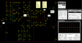
I've surprised myself. The schematic achieves incredibly low THD. Sub ppm numbers at 20KHz, 200W into 4 ohm resistive. It wasn't an easy way to get there though. I initially set off using ideal current sources and went on by implementing each of them carefully with the goal to stay in the low distortion region. I've got one more ideal CS to go.
Here are some numbers:
I think, even for a simulated schematic, having achieved these numbers into the given load are quite a feat. I definitely intend to build this amp and let my ears be the final judge - but so far, in the numerical domain this amp seems to be a real gem. I am confident that when actually built, the numbers won't be far off - the intrinsic performance isn't much dependant on actual component values. I can state this based on my previous project that showed numbers actually much better than I got in the simulator. I attribute that to the fact that in real, the analog resolution is infinite unlike in a simulator and as a result, would induce artifacts in simulation data. All in all, I'd like to stress that these simulation results are not holy, they are a guidance.
Anyways, the amp is still in its design stage. Once I've completed the final current source (that of the LTP), I'll work towards a prototype and see how it turns out for real. Given my previous experience with creating an amp from simulation to a real, working prototype, this new design is very promising!
I'll be glad to answer questions about the design and otherwise discuss its various aspects.
Note: The original schema in the post was designed for 200W; as the design progressed I scaled up the power to its intended target of 500W into 4 Ohms.
SOM200 - Ultra Low Distortion Pure FET Power Amplifier
Hello everyone!
I promised to give my amp its own thread when I had finished the initial design, but in order not to clutter a different thread, I'll do so now.
I've been designing amps for a while now and while my latests creation has turned out rather well I was inspired by the JFET input, MOSFET VAS, LATERAL output = Perfect!! to design an all-FET power amp.
The goal of this design was to achieve and keep a low THD as development continues. Through careful analysis I've been able to figure out optimal design parameters for each of the amp's sub circuits like IPS, current mirrors, VAS, CCS' and so on.
I've surprised myself. The schematic achieves incredibly low THD. Sub ppm numbers at 20KHz, 200W into 4 ohm resistive. It wasn't an easy way to get there though. I initially set off using ideal current sources and went on by implementing each of them carefully with the goal to stay in the low distortion region. I've got one more ideal CS to go.
Here are some numbers:
Code:
Fourier analysis for $out:
DC component: -8.1332e-007
  No. Harmonics: 20, THD: 1.06368e-005 %, Gridsize: 512, Interpolation Degree: 1
Harmonic Frequency    Magnitude    Phase        Norm. Mag    Norm. Phase
-------- ---------    ---------    -----        ---------    -----------
 1       1000         40.017       -0.018774    1            0
 2       2000         8.39746e-008 -41.014      2.09847e-009 -40.995
 3       3000         7.74366e-007 -164.39      1.93509e-008 -164.37
 4       4000         3.71717e-008 -67.983      9.28897e-010 -67.964
 5       5000         2.47765e-007 19.1049      6.19148e-009 19.1236
 6       6000         6.07316e-008 -42.895      1.51764e-009 -42.877
 7       7000         1.8439e-007  -79.51       4.60778e-009 -79.491
 8       8000         3.93825e-008 -4.7429      9.84143e-010 -4.7242
 9       9000         2.86322e-007 108.143      7.15501e-009 108.162
 10      10000        6.94968e-008 42.6485      1.73668e-009 42.6673
 11      11000        2.09569e-006 -34.091      5.23699e-008 -34.072
 12      12000        5.89009e-007 89.7746      1.4719e-008  89.7933
 13      13000        4.59748e-007 -56.343      1.14888e-008 -56.324
 14      14000        7.11066e-007 -149.87      1.77691e-008 -149.85
 15      15000        3.39956e-006 -32.858      8.49528e-008 -32.839
 16      16000        2.0638e-007  -113.63      5.15732e-009 -113.61
 17      17000        4.31867e-007 -160.95      1.07921e-008 -160.93
 18      18000        1.64712e-007 -101.73      4.11605e-009 -101.71
 19      19000        1.7081e-007  -39.923      4.26844e-009 -39.905
 20      20000        1.55652e-007 -87.785      3.88966e-009 -87.766
Code:
Fourier analysis for $out:
DC component: 6.14164e-006
  No. Harmonics: 10, THD: 8.37035e-005 %, Gridsize: 256, Interpolation Degree: 1
Harmonic Frequency    Magnitude    Phase        Norm. Mag    Norm. Phase
-------- ---------    ---------    -----        ---------    -----------
 1       20000        40.0087      -0.3756      1            0
 2       40000        4.66297e-006 -86.343      1.16549e-007 -85.967
 3       60000        2.26497e-005 8.36849      5.66119e-007 8.74409
 4       80000        7.37226e-006 89.176       1.84267e-007 89.5516
 5       100000       2.23136e-005 4.16724      5.5772e-007  4.54284
 6       120000       5.57379e-007 132.186      1.39315e-008 132.561
 7       140000       1.59006e-006 43.1607      3.97429e-008 43.5363
 8       160000       3.54731e-006 92.0763      8.86634e-008 92.4519
 9       180000       3.17283e-006 0.633482     7.93036e-008 1.00908
 10      200000       3.0004e-006  96.2616      7.49938e-008 96.6372
I think, even for a simulated schematic, having achieved these numbers into the given load are quite a feat. I definitely intend to build this amp and let my ears be the final judge - but so far, in the numerical domain this amp seems to be a real gem. I am confident that when actually built, the numbers won't be far off - the intrinsic performance isn't much dependant on actual component values. I can state this based on my previous project that showed numbers actually much better than I got in the simulator. I attribute that to the fact that in real, the analog resolution is infinite unlike in a simulator and as a result, would induce artifacts in simulation data. All in all, I'd like to stress that these simulation results are not holy, they are a guidance.
Anyways, the amp is still in its design stage. Once I've completed the final current source (that of the LTP), I'll work towards a prototype and see how it turns out for real. Given my previous experience with creating an amp from simulation to a real, working prototype, this new design is very promising!
I'll be glad to answer questions about the design and otherwise discuss its various aspects.
Attachments
Last edited:
Hi Adrew, thanks for asking. Yeah, the two combinations Q3, Q4, R3, C20 and Q16, Q17, R28, C19 are two tracking cascodes. I could do with only one set if it wasn't for the relatively high IPS current, ~ 10mA in each leg of the LTP. The second set is merely to divide the supply voltage. it allows to set the Vds for the JFETs and the second sets the Vds for the first cascode. Here, tracking means that the JFETs see a constant Vds because the cascodes are referenced against the JFET sources.
Q10 in the VAS is also a tracking cascode although here it tracks the the VAS device (Q11) drive. It is biased by R14. R4, R14 and Q7 run approximately 2mA when in equibrilium and C2 bypasses the cascode bias R14 so that for AC signals, Q11 remains the controlling device rather than Q10. Since Q7 doesn't run much current, its drain did not have to go through the cascode and could directly connect to the VAS output. So basically, the source follower FET Q7 also provides a 'moving' BIAS for its cascode rather than running the cascode off an external voltage reference. The cascode's Vgs as a result of its current is no longer 'bouncing' off a fixed reference, impeding linearity but instead gets moved along by the drive of the VAS device.
It may sound complex and crazy, but simulations proved this topology to be much better than a fixed reference cascode.
The VAS current is about 15mA. It's set by JFET Q13 in the CCS for the VAS. Here I've used a current mirror to in order to replace the JFET load with a fixed reference cascode Q18 as the CCS output cascode Q12 is subject to voltage swings over its drain. It makes for a great performning CCS I think.
 i think i'll wait till i have a bit more working knowledge behind me before i attempt to build such a thing, but the ccs sounds quite intriguing
Hi Magicbox
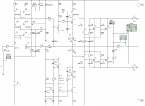
Interesting the design has become a bit more complex. Could you perhaps show the schematic with a white background, I find it hard to follow with my laptop.
I'll add a black on white schematic for convenience. Unfortunately yes, the schematic became a little more complex mainly because I wanted to shoot for a higher power output which resulted in an extra cascode set in the IPS and a cascode for the VAS. And not unsignificantly, two ideal CS' have now been implemented as well.
Other than that, the base schematic should still be recognizable. The only thing that changed compared to the base schematic is that the drain of the source follower FET is no longer connected to GND, but directly to the VAS north-side. Having given the VAS a higer Iq, it is fast enough to drive a much larger voltage swing
")
You'll find a black-on-white schematic attached to this post.
Attachments
Last edited:
Magicbox, well I take my hats off, Ive been a member here for over 5 years and your tracking cascode is only the second significant development Ive seen here. Other designs around here are mostly what has been done for the last 30 years with a little tweak here and there but the basics remain the same. Edmond Stuart s TMC was the first. Kenpeter and Elvee are two other members thinking out of the box and come up with some inovative ideas never seen or used before.
Ignoring all the current sources (I prefer simple circuits) I find your vas most excellent indeed. If you dont mind Im going to make a comparison with my idea, I think the two will be very close in comparison, as the principle is very much the same, I just did it a little different and name it something else. One can do magic with Mosfets if you can think outside the box.
Very noble of you to show it here, if patents werent so useless as its very difficult to patrol and costly too, it would be the wise way for you to go.
Interesting.
You might find that the THD e.a. numbers go up a bit when you replace that 23mA current source with real components, though....
Yes, it does. But the critical job for this CS is to make sure the current through each JFET biasses them just below their forward bias point. Too few / too much current degrades performance. I've found the sweet spot to be around a Vgs of 0V, ever so slightly negative.
Knowing this, I have to make this CS in such way I can reasonably adjust it without introducing too much noise into the circuit. I plan to do this with a current mirror so I can use a high voltage for a regular source follower with an adjustable input voltage. I'll figure out a way
similar to the Pass B1 and Curl.JFET biasses them just below their forward bias point. Too few / too much current degrades performance. I've found the sweet spot to be around a Vgs of 0V, ever so slightly negative.
You honour me by putting me on the same shelf as these guys with respect to 'inventing' topologies. I've seen threads of them and they seem very knowledgable guys and I wouldn't put myself in the same ball park as themMagicbox, well I take my hats off, Ive been a member here for over 5 years and your tracking cascode is only the second significant development Ive seen here. Other designs around here are mostly what has been done for the last 30 years with a little tweak here and there but the basics remain the same. Edmond Stuart s TMC was the first. Kenpeter and Elvee are two other members thinking out of the box and come up with some inovative ideas never seen or used before.
Thanks once more. I wouldn't suspect the tracking cascode to be patent worthy, let alone whether something like that has been patended or not in the first place. In any case, it's there for everyone to to use and try and see if their designs improve because of it. Feel free to compare it with your conceptsIgnoring all the current sources (I prefer simple circuits) I find your vas most excellent indeed. If you dont mind Im going to make a comparison with my idea, I think the two will be very close in comparison, as the principle is very much the same, I just did it a little different and name it something else. One can do magic with Mosfets if you can think outside the box.
Very noble of you to show it here, if patents werent so useless as its very difficult to patrol and costly too, it would be the wise way for you to go.
So far I'm quite happy with the design, having been able to keep numbers in the same ball park after having transformed two ideal CS' into actual discrete currentsources. Although I have to admit that the VAS current source took some effort to obtain these results.
The final current source is also going to be a challenge in that it needs to be adjustable without causing additional noise to the circuit.
Dont be so modest, look around the forum, always the same circuits in different guises or what has been used and forgotten and then reinvented or re discovered again. This works, anyway your vas isnt patented but you can find several papers dealing with various cascode ideas with mosfets, the earliest Ive seen dates from 1990 and all have been with ideas relating to microprocesor development, I used one of these ideas as basis too. Like I said no patents were ever filed for these cascodes. They outperform conventional cascodes by a large margin and in many ways.
Magicbox, well I take my hats off, Ive been a member here for over 5 years and your tracking cascode is only the second significant development Ive seen here.
I think Erno Borbely invented tracking cascode (If I understand tracking cascode is the one keeping constant Vds on lower device). I was using such cascodes in discrete opamps by Erno (I was using LEDs for this type of biasing - because I was unable to find devices with high enough Vgs). Here we can see great way to set custom Vds and keep it constant in the simple way and here is the great way for high voltage stages. What is more this is pretty straight forward to implement and really scale able.
Great design!
Last edited:
Magicbox,
If you'd like a simple way to implement a tracking cascode for the input JFETs, then the attached circuit is about as simple as you can get. It's not my idea, or new, I remember Ed Cherry showing it to me about 30 years ago.
The DN2530 (and also DN2540) depletion mode Mosfets can be used to implement very good constant current sources (CCS), and unlike LED biased BJTs, they don't `stick' when driven into overload. The FETzilla amp uses a bootstrapped DN2530 for the VAS CCS, which also works very well (see the FETzilla thread in the AKSA forum).
Paul Bysouth, Nov 2011
Attachments
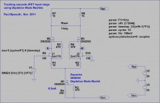
I think I prefer the use of an auxilary current source to implement the tracking cascode for the JFETs. While using depletion FETs is a nice way to keep parts count down, it's not flexible in that you can't 'program' the Vds for the JFETs, you're tied to the Vgs drop of the dep. FETs. Using a currentsource makes it easy to still reference regular fets against the JFET sources, though through a resistor you can easily set your desired Vds for the JFETs for optimal performance The bottom CCS will just sink the auxilary CCS and splits the remainder between the two LTP legs.
However, the VAS cascode is differently and while you guys comment on the input cascode, the VAS cascode didn't receive similar attention while I believe it's that cascode topology that's a bit different than what you'd normally see.
LazyCat, when you look at the schematic, what do you think? Ofcourse it's near impossible to tell audio performance from a plain schematic, could you give any hint at the level of 'promising' for this design?
The bottom CCS will just sink the auxilary CCS and splits the remainder between the two LTP legs.However, the VAS cascode is differently and while you guys comment on the input cascode, the VAS cascode didn't receive similar attention while I believe it's that cascode topology that's a bit different than what you'd normally see.
LazyCat, when you look at the schematic, what do you think? Ofcourse it's near impossible to tell audio performance from a plain schematic, could you give any hint at the level of 'promising' for this design?
Well, since part of the design has been about scalability, I've upscaled it to 500W into 4Ohms which was fairly easy to do. No additional part counts, just different bias values. It still achieves ~ 1ppm for THD20! Oh, I lied about the parts count: The OPS has been doubled, 4 pairs of output FETs now.
That configuration is similar to the '86 "Kilowatter" 1KW hifi amp published by Elector. I've built it and has served me for many years. However, I'm working on a revision that should yield much better specs than the original. I first built a 80W FET amp based on the Kilowatter topology but with a totally reworked VAS and while performance of the new design was a significant improvement over the original schematic, I'm still not going to use that as a base for the revision. Instead, I'll be using the design as presented in this thread. I'm convinced by the convenience and performance of a single-ended setup while the previous design was a symmetrical design.
The upscaling of this design turns out very well!
- Status
- This old topic is closed. If you want to reopen this topic, contact a moderator using the "Report Post" button.
- Home
- Amplifiers
- Solid State
- "State-Of-MOS": 200W Ultra Low Distortion Pure FET Amplifier