have a couple questions for anyone who is experienced in amp design.
I have been looking through various circuits on the web for MOSFET based power amps. I have been looking at class AB source follower type designs and have a couple questions.
First:
Suppose a MOSFET output stage uses an IRFP240 and IRFP9240 for the output devices in class AB setup. There is approx. 4 volts needed from gate to source to bias the devices. In addtion to that you need your command signal to command different levels of current through the FET. Since, the gate voltage needed to get current through the FET is referenced to the Source of the device (Vgs), really your AC command signal to the power stage must be referenced to the OUTPUT of the the P-channel/N-channel output pair, not to ground
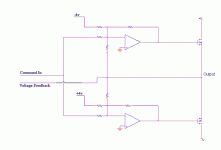
So, My question is, what is the easiest way of referencing a signal to the output of the amp and not Ground? Is it possible to use a Power OP amp such as the LM3886 for easy gate drive? I have attached a simplfied schematic of a possible gate drive with the LM3886. I have left out stability components for clarity. This circuit uses two power op-amps; one for each gate. The op-amps are in a basic summing confuration. The command signal is summed with a gate bias offset voltage (its the opposite polarity because the summer circuit will invert). THe output voltage is summed back in with the bias voltage and the command. THis way the gate voltage will always be above the output voltage by the bias voltage plus the command signal. The Voltage feedback from the output could also then be fed back into an LTP or other input circuit for the global feedback.
Is this circuit too absurd? My background is in embedded software and this is my first attempt at a power amp. This seemed to make sense to me. Some of the descrete circuits I saw seemed very complex. If anyone has a good website on linear FET drive please give me a link.
My second question. Even though most people claim that the IRFP240 and IRFP9240 are a matched pair, this to me seems like a stretch of the truth. I notice that they both have different values for transconductance(4.2siemens and 6.9 siemens). In a class AB configuration wont the mis-matched Transconductances cause an assymetrical output?? I know negative feedback can compensate for this but is there a simple way to get rid of this problem before global negative feedback is applied?
MOSFET Experts, Please give me some tips. I like using them for switches more than linear power stages.
I have been looking through various circuits on the web for MOSFET based power amps. I have been looking at class AB source follower type designs and have a couple questions.
First:
Suppose a MOSFET output stage uses an IRFP240 and IRFP9240 for the output devices in class AB setup. There is approx. 4 volts needed from gate to source to bias the devices. In addtion to that you need your command signal to command different levels of current through the FET. Since, the gate voltage needed to get current through the FET is referenced to the Source of the device (Vgs), really your AC command signal to the power stage must be referenced to the OUTPUT of the the P-channel/N-channel output pair, not to ground
So, My question is, what is the easiest way of referencing a signal to the output of the amp and not Ground? Is it possible to use a Power OP amp such as the LM3886 for easy gate drive? I have attached a simplfied schematic of a possible gate drive with the LM3886. I have left out stability components for clarity. This circuit uses two power op-amps; one for each gate. The op-amps are in a basic summing confuration. The command signal is summed with a gate bias offset voltage (its the opposite polarity because the summer circuit will invert). THe output voltage is summed back in with the bias voltage and the command. THis way the gate voltage will always be above the output voltage by the bias voltage plus the command signal. The Voltage feedback from the output could also then be fed back into an LTP or other input circuit for the global feedback.
Is this circuit too absurd? My background is in embedded software and this is my first attempt at a power amp. This seemed to make sense to me. Some of the descrete circuits I saw seemed very complex. If anyone has a good website on linear FET drive please give me a link.
My second question. Even though most people claim that the IRFP240 and IRFP9240 are a matched pair, this to me seems like a stretch of the truth. I notice that they both have different values for transconductance(4.2siemens and 6.9 siemens). In a class AB configuration wont the mis-matched Transconductances cause an assymetrical output?? I know negative feedback can compensate for this but is there a simple way to get rid of this problem before global negative feedback is applied?
MOSFET Experts, Please give me some tips. I like using them for switches more than linear power stages.
Attachments
hugeli60, the key is that you said that you will be using them for switches. In that case, things may be much easier and more efficient if you use the IR2110 or IR2113 to drive each half of a totem pole. One chip can drive an upper and lower transistor with ease. Not only that, the chip is designed to drive only N-channel transistors. Therefore, you can have matched performance for the upper and lower halves. The greatest benefit besides the chip's ability to pulse up to 2 amps of current for quick switching, is the ability of the chip to take both inputs referenced to the negative power supply rail and drive both gates with only 5 volt pulses if you drive them from digital circuitry and make the input portion of the chip run off of 5v. Alternately, you can pulse the inputs with drive signals up to 15 volts (20 max).
http://www.irf.com/product-info/datasheets/data/ir2110.pdf
The IR2110/3 can only maintain the output condition either high or low. That could be one drawback for it working out for you.
http://www.irf.com/product-info/datasheets/data/ir2110.pdf
The IR2110/3 can only maintain the output condition either high or low. That could be one drawback for it working out for you.
"The IR2110/3 can only maintain the output condition either high or low. That could be one drawback for it working out for you."
I meant to say that it can cause the outputs to go either high or low or high impedance. And for your second question, the reason for the performance difference is that the P-channel devices do not have the same intrinsic properties as the N-channel. That is one reason why they are not made for voltages over around 200v.
I meant to say that it can cause the outputs to go either high or low or high impedance. And for your second question, the reason for the performance difference is that the P-channel devices do not have the same intrinsic properties as the N-channel. That is one reason why they are not made for voltages over around 200v.
I am aware of the 2113 Chip. I want to use these fet for a Linear Power Amp. It sounds to me like your describing a setup for a Class-D full Bridge switcher. Am I interpretting you correctly? I have about 25 of these fets (IRFP9240 and IRFP240) and I want to use them in a linear amp design. My next project will be a class D switcher but I want to do some linear stuff first.
My statement about using the MOSFETS for switches was somewhat misleading. I like to USE MOSFETS in switch applications, not for linear applications. But in this case I have alot of these MOSFETS in inventory and I want to use them in a linear amp. I believe some of the old carvin amps used these devices
Oh, cool. I do like the principle of what you are doing driving the mosfets with the amp chips. You should have enough drive to attain a fast slew rate. I like the elegance of the idea of using the summing circuit, but I can't verify that will work out.
You are right about the Class-D full Bridge switcher. That configuration is currently the exact project I am working on. I have decided to attemp a setup where the transistor switchings between the two legs are nominally in phase while the audio is inverted before going into one side. Hopefully, this scheme will overcome the problem of so much filtering being needed in the load circuit. That filtering has been consuming much power in some designs I have experimented with.
You are right about the Class-D full Bridge switcher. That configuration is currently the exact project I am working on. I have decided to attemp a setup where the transistor switchings between the two legs are nominally in phase while the audio is inverted before going into one side. Hopefully, this scheme will overcome the problem of so much filtering being needed in the load circuit. That filtering has been consuming much power in some designs I have experimented with.
hugeli60,
If you reference the drive signal(s) to the output node, you'll be operating the IRFP240/9240 as a transconductance stage rather than as a follower. You could do it, but that's different from what's generally described in DIY articles using these MOSFETs.
The usual way to operate the output stage as a follower is to reference the drive signal to ground, rather than to the output. This means that the drive signal has to swing as least as much voltage as the expected output signal, and usually several volts more than that.
Also, when using IR type MOSFETs, the +/-4V bias is most often derived from an adjustable temperature compensated bias voltage source (e.g. another IR type MOSFET) tied across the gates of the output pair.
The irf240/9240 are not identical just as u stated,the transconductance is different as well as the input capacitance. I've used them in out stages without loop NFB and had to use two P-devices(irf9240) and one N-device(irf240) which basically gave me two complementary devices(treat two irf9240s as one 240). I don't use drive stages, and the bias at the gainstage is 14mA, and the amp is flat to about 50kHz.
Because of the differences in N-devices and P-devices, I've designed output stages which only uses N-devices, and with two irf240s I get flat responses to about 150kHz, and about 50watts of power(without loop NFB). I use this in a balanced setup, or bridge if u prefer, and get about 150watts with four N-devices total.
I'd skip the opamp as driver. Look at Nelson Pass' mod of the push-pull bipolar amp, can't remember the name of it, but it's the one where he replaces the output with MOSFETs. Its a good amp, and can be modded to your wishes. I'd make something like it with all the gain set at input/drive stage and not use loop NFB to set gain.
..I can't help it, I just don't like loop NFB...
regards, Nick.
forgot..
...the drive voltage, which needs to be about five volts higher than the max outputswing. So if you want a 50watter for instance, the output stage's rails should be ruffly +/-25volts, and the input/drive stage should have+/-30volts or so. Since u should use seperate trannies for the in/out stage, u might as well give the instage some headroom and go for +/- 40volts. That'll enable the input/drive stage to drive the output to it's max output rating.
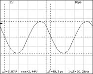
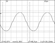
btw: I have scope pics of the output stage using one each n and p-device, and using one n-device and two p-devices, which shows the difference it makes. How can i post them here?
regards, Nick
...the drive voltage, which needs to be about five volts higher than the max outputswing. So if you want a 50watter for instance, the output stage's rails should be ruffly +/-25volts, and the input/drive stage should have+/-30volts or so. Since u should use seperate trannies for the in/out stage, u might as well give the instage some headroom and go for +/- 40volts. That'll enable the input/drive stage to drive the output to it's max output rating.
btw: I have scope pics of the output stage using one each n and p-device, and using one n-device and two p-devices, which shows the difference it makes. How can i post them here?
regards, Nick
Attachments
just to clearify...
the stages are biased low, both at only a few mA, and no loop NFB is used. The load is an 8ohm pwr resistor. The pic of the stage using one each devices looks simply like it's biased too low, and we see the x-over distortion, which actually is the case, but the 'two P- one N-device' stage is biased just as low, and tho it too has high distortion, it surely demonstrates the difference it makes when the N- and P-devices are more equal in transconductance. Both stages sound very well when the bias is set above 100mA even without loop NFB.
the stages are biased low, both at only a few mA, and no loop NFB is used. The load is an 8ohm pwr resistor. The pic of the stage using one each devices looks simply like it's biased too low, and we see the x-over distortion, which actually is the case, but the 'two P- one N-device' stage is biased just as low, and tho it too has high distortion, it surely demonstrates the difference it makes when the N- and P-devices are more equal in transconductance. Both stages sound very well when the bias is set above 100mA even without loop NFB.
SemperFi said:I've designed output stages which only uses N-devices, and with two irf240s I get flat responses to about 150kHz, and about 50watts of power(without loop NFB). I use this in a balanced setup, or bridge if u prefer, and get about 150watts with four N-devices total.
Nick,
I'd be interested in details of your 50W N-MOS bridge setup if you care to share them. If you have a lot to say, and think if would be of general interest, you can always start a new thread on the topic.
")
okey
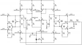
Here's a ruff version, meaning some values are modded slightly. The feedback network R25,R26, and C1 are for DC offset only, signal wise the amp is zero-loop NFB. The DC NFB network is also at other output(both), but I only have the demo version of this circuit CAD so ran out of available parts allowed.
R16 and R20 are pots, so bias is eaier to adjust.
The input stage has about 10volts higher rails than output. I've also done it with bipolars in the CCS and mirrors, haven't decided which I prefer yet.
The gain as shown is about 30dB into 8ohms.
Sounds great with 100mA bias.
I'll probably include this with PCB layout on my website soon.
Regards, Nick
Attachments
Nick, thanks for posting the schematic. About your output stage, it looks like the upper MOSFET(s) might be set up to act like a partial CCS at low output currents, then transition to (quasi) complementary behavior at higher levels. Is that how it works out in practice? I've modeled some circuits that work that way, but never actually built any. In any case, I definitely think you should add this one to your web site when you get the time.
- Status
- This old topic is closed. If you want to reopen this topic, contact a moderator using the "Report Post" button.
- Home
- Amplifiers
- Solid State
- MOSFET Drive help