Status:
I've made two prototype boards:
- board 1: diff input pair +ccs + vas
- board 2: drivers (2SK2013/2SJ313/ + vbe multiplier + OPS (on old copper clad)
What have I done:
- Made board 1 and choosen the right resistor value for the biasing of the diff input pair. All voltages and currents looked good.
- Made board two with 1output pair soldered directly to the board.
- powered everything on with 10Ohm resistors instead of the fuses
- all measured good and set the bias current
- hooked up a speaker and an input signal
- and we had music,")
BUT then:
- I've used a second output pair
- used wires with a lenght of 20mm between board and output FET's.
- Gate stoppers of 220Ohm are mounted on the board.
- Powered it on and measuring continous the bias current.
==> I saw that bias current keeps rising, I pulled the plug and recheckt everything, no error found.
- Then, turnen bias current to minimum
- Powered it on and increasing bias current , once I got to +-100mA the bias current keeps rising!?
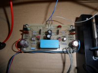
- I desoldered everything and soldered the FET's directly to the board (see picture below)
- Now I can set the bias current to a fixed value, but I noticed that the bias current between the four FET's are varying a lot (from 100mA - 400mA)?
Question:
Could it be that due to the wires of 20mm between board and output FET's (2SK1530 / 2SJ20), the FET's destroid them selves due to oscillation?
I've made two prototype boards:
- board 1: diff input pair +ccs + vas
- board 2: drivers (2SK2013/2SJ313/ + vbe multiplier + OPS (on old copper clad)
What have I done:
- Made board 1 and choosen the right resistor value for the biasing of the diff input pair. All voltages and currents looked good.
- Made board two with 1output pair soldered directly to the board.
- powered everything on with 10Ohm resistors instead of the fuses
- all measured good and set the bias current
- hooked up a speaker and an input signal
- and we had music,
BUT then:
- I've used a second output pair
- used wires with a lenght of 20mm between board and output FET's.
- Gate stoppers of 220Ohm are mounted on the board.
- Powered it on and measuring continous the bias current.
==> I saw that bias current keeps rising, I pulled the plug and recheckt everything, no error found.
- Then, turnen bias current to minimum
- Powered it on and increasing bias current , once I got to +-100mA the bias current keeps rising!?
- I desoldered everything and soldered the FET's directly to the board (see picture below)
- Now I can set the bias current to a fixed value, but I noticed that the bias current between the four FET's are varying a lot (from 100mA - 400mA)?
Question:
Could it be that due to the wires of 20mm between board and output FET's (2SK1530 / 2SJ20), the FET's destroid them selves due to oscillation?
Attachments
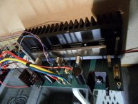
Does the right hand pic show a 5th transistor trapped behind the clamp bar?
Is that the heatsink located Vbe multiplier? Is the Vbe transistor actually in thermal contact with the heatsink?
Is a two bolt fixing for the clamp plate, sufficient to ensure all four output devices are in flat contact with the heatsink? I recommend a five bolt fixing for four output devices.
Is that the heatsink located Vbe multiplier? Is the Vbe transistor actually in thermal contact with the heatsink?
Is a two bolt fixing for the clamp plate, sufficient to ensure all four output devices are in flat contact with the heatsink? I recommend a five bolt fixing for four output devices.
Hi Andrew,
Yes, behind the bar is a2SK792 FET for the bias setting, it is pressed to the heatsink with the same bar.
The board as you see it (blue/green material) the heatsink and mounting of the output fet's is only temporary for testing purposes. Once everything is finetuned, new PCB will be made and each FET will have its own bolt for connecting to the heatsink.
My guess is that it's not he VBE multiplier which is defect, because the bias current rises +- 5mA/second.
Greetz
Have you tried moving the Vbe multiplier transistor?
With the two bolts located as in the pic, the tighter you make the bolts the less clamping force on the Vbe multiplier.
It could be quite loose or not in thermal contact. Is the Vbe the same thickness as the output devices?
With the two bolts located as in the pic, the tighter you make the bolts the less clamping force on the Vbe multiplier.
It could be quite loose or not in thermal contact. Is the Vbe the same thickness as the output devices?
But how can one than explain that before this happened, the four ouput FET's measured the same bias current. The situation now is that, 1 FET measures 80mA, the second 400mA, the 3th 200mA and the 4th 120mA?
I have four new Fet's laying I'll try these tommorow, but then directly soldered to the pcb.
I have four new Fet's laying I'll try these tommorow, but then directly soldered to the pcb.
I'ts running again but unstable bias
I removed the output FETS and placed 2 1K resistors instead, this to keep the NFB network.
I measured all voltages/current, everything looked fine.
I mounted 2 new output FET's, but this time close the PCB and the gatestopper right at the legs of the FET's.
I powered it on, and yes, all measured fine.
Than I started following the bias current throught the OPS.
Cold amp: Set bias current at 180mA
Warm Amp (40°C): Bias current dropped to 140mA
Than increased bias with trimpot back to 180mA
Amp cooled down again: Bias measured 215mA
The VGS multiplier is overcompensated. I'm using a 2SK792 FET instead of the irf9410 in the schematic. The resistor values in the schematic are the same as in practice.
What should I do to improve it?
Attachments
How much did the bias voltage vary when the outputs were disconnected?
You can reduce temp comp by various additions to the multiplier.
The easiest is to add a resistor to the emitter of the Vbe transistor.
I like to see a small droop in output bias current as temperature rises to maximum.
I see this as compensating for extra warm weather conditions or hard driving operation.
This over-compensation is frowned upon by the purists. But I consider a working amplifier to be better than one that has just blown up and produces no sound after the explosion.
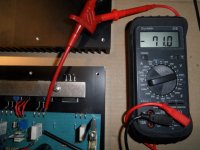
After I desoldered them, I've measured V-bias 7.9V. This is the correct value which I presetted when the Fet's where still running.
I tried several resistors in the emitter, even with a 100Ohm resistor the bias current keeps dropping the same as without the extra resistor.
I've red somewhere on the forum that 100Ohm is about the max to put here (reason for this??), with a current of +-2.2mA through the bias spreader this is 0.22V, this is low compared to the Vgs of the Fet used (about 2V). Now, I've putted a 1N4148 diode in the emitter, I'm testing this at this moment, with this extra 0.6V, the multiplication factor is smaller and the error should become normally smaller also.
Yes, overcompensation is safe, have you a rule of thumb what the variation of a bias spreader may or could be.
Last edited:
Hi,
I don't have a rule of thumb.
What I will do as part of my initial testing is check for over or under compensation.
I will not accept a ClassAB amp that biases itself higher as temperature rises above normal working temp.
If Vgs is 2V, then Vbias at the Gates will be 4V.
Where is that 7.9V measured relative to the FET Gates?
I don't have a rule of thumb.
What I will do as part of my initial testing is check for over or under compensation.
I will not accept a ClassAB amp that biases itself higher as temperature rises above normal working temp.
this does not sound right.I've measured V-bias 7.9V. This is the correct value which I presetted ................ this is low compared to the Vgs of the Fet used (about 2V).
If Vgs is 2V, then Vbias at the Gates will be 4V.
Where is that 7.9V measured relative to the FET Gates?
Last edited:
Oops,
The 7.9V is measured over the VGS multiplier. Between the Gates of the Ouput fets, I have indeed 4Volts.
Regarding the 1N4148:
By cool heatsink at start up: bias rises to 75mV = 227mA
When amp starts getting hotter: bias decreased to 60mV = 182mA
==> Variation of 20%
Without anything in the emitter I had approx the same experience.
==> Placing a resistor or Diode in the emitter doesn't have the result I hoped for.
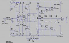
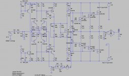
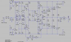
This is the current shematic, the IRFP9410 is in practice 2SK792.
Due to the fact that I'm running the Drivers (2SK2013/2SJ313) in a very non-lineaur region (when looking at the ID/Vgs curve)), the change in Vgs of the drivers comming from the VGS-multiplier has a second impact on the bias current throug the OPS.
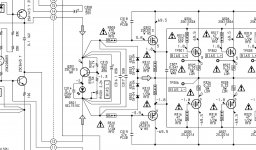
Apparently, Sony is using the same driver and output FET's in some of there amps. See the second attachment. In the Sony TA-N1, the drivers are also mounted on smaller heatsinks.
I think I'm gonna try this Vbe multiplier.
Greetz
Due to the fact that I'm running the Drivers (2SK2013/2SJ313) in a very non-lineaur region (when looking at the ID/Vgs curve)), the change in Vgs of the drivers comming from the VGS-multiplier has a second impact on the bias current throug the OPS.
Apparently, Sony is using the same driver and output FET's in some of there amps. See the second attachment. In the Sony TA-N1, the drivers are also mounted on smaller heatsinks.
I think I'm gonna try this Vbe multiplier.
Greetz
Attachments
The diode in the emitter circuit of a BJT multiplier has an effect.
Putting that same 600mV to 700mV drop into the source circuit of the FET multiplier may have a much smaller effect. 650:650mV as against 650:3500mV
Does your VAS current change as the amplifier warms up from cold, to operating quiescent, to very hot loud music sessions?
D.Self showed how to stabilise the multiplier output voltage when multiplier current varied for a BJT version.
I don't know how to apply that compensation to a FET version. It would be easy to set up a plug board experiment to find what resistor values show that compensating effect.
Borbely used 2SJ79/2SK216 as output stage driver. For VAS the 2sK2013/2sJ313 as the cascode devices in a Hawksford cascode with 2 x 2sj74/2sk170 in parrallel as the VAS gain devices to obtain 16 ma VAS current in his last Millenium amplifiers. He used 2sk216 as bias spreader.
Last edited:
Drivers:
Thanks, and yes I was aware of this. One reason wy I've choosen for the 313/2013 devices is to learn them better for an other project, where I'm using 5pairs of 2SC2292/2SA1216 as OPS. The 2SK216/2SJ79 devices have not enough current capability to drive these.
VBE/VGS-multiplier:
I've tried almost 10 different variations. The best sofar is using a 2SC2911 transistor with two red-leds in the emitter. The bias spread is only 10mA for heatsink temperature difference of 30°C.
At the moment I'm for 3weeks in Tianjin (China), no possibility to do more tests.
Review Vbe multiplier
At this moment the 2SC2922 with 2 red led's in the emitter has the best results.
It is very slightly overcompensated.
Cold amp: 180mA
Amp at stable temp: +-30°C: 175mA
An other test I did:
I've used my frequency generator as input signal and measured the Vbe in function of the input frequency. From 50Hz to 20kHz I measured no difference, value stayed at 7.74V.
I haven't seen a Vbe multiplier with such a big "voltage" (2x 1.52V) added in the emitter, this is wy I'm asking if anybody has some remarks about this.
Attachments
- Status
- This old topic is closed. If you want to reopen this topic, contact a moderator using the "Report Post" button.
- Home
- Amplifiers
- Solid State
- Amp design for subwoofer and wideband duty