By analogy with predistortion, one could call this postdistortion. As there is no comparison, even indirectly, with the original input signal it is not feedback. It could be argued that the active load does not use feedback but attenuation. This is because the current through the load is determined by the upper FET transconductance function being fed an attenuated copy of the output voltage; there is no feedback to linearise this current, indeed that would be counterproductive. The only glimpse of feedback comes from the upper FETs own drain-source impedance, but SET fans tells us that this should not be considered as feeback!
We can argue ad infinitum how to call it, however the mechanism involved is usually called "indirect feedback" - that is, the output signal is fed back not to the signal input, but to another - "feedback" input and the resulting currents are added to produce the output. Examples of this technique can be found in some ICs circuitry.
Cheers
Alex
Last edited:
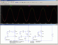
I've tried to simulate the circut: as far I've found the mu-follower configuration has much less distorsion than the Indirect feedback.
This circuit works well if the conditions that MarcelvdG has outlined a bit earlier are fulfilled. For low-gain devices (i.e. valve triodes) the mu-follower configuration would work better.
Cheers
Alex
The most common type of indirect feedback circuit used in integrated circuits is the current mirror. You can regard a current mirror as a current amplifier with indirect feedback, as a circuit using compensation, as a circuit using predistortion or as a rather simple translinear loop. No matter how you look at it, it works.
Indirect voltage feedback is sometimes used for instrumentation amplifiers. Apply the input signal to one differential pair and the (attenuated) output signal to a matching differential pair, and add a loop amplifier that nulls the difference between the output signals of the differential pairs. I've used this once for a discrete audio circuit, see the attachment (symmetrical unity gain buffer that can be used for converting differential signals to single-ended and vice versa).
Alex's circuit is similar to the indirect voltage feedback instrumentation amplifier, except that he has replaced the differential pairs with JFET's and the loop amplifier with a wire. That is, the JFET's themselves are to produce enough loop gain.
Attachments
The most common type of indirect feedback circuit used in integrated circuits is the current mirror. You can regard a current mirror as a current amplifier with indirect feedback, as a circuit using compensation, as a circuit using predistortion or as a rather simple translinear loop. No matter how you look at it, it works.
Indirect voltage feedback is sometimes used for instrumentation amplifiers. Apply the input signal to one differential pair and the (attenuated) output signal to a matching differential pair, and add a loop amplifier that nulls the difference between the output signals of the differential pairs. I've used this once for a discrete audio circuit, see the attachment (symmetrical unity gain buffer that can be used for converting differential signals to single-ended and vice versa).
Alex's circuit is similar to the indirect voltage feedback instrumentation amplifier, except that he has replaced the differential pairs with JFET's and the loop amplifier with a wire. That is, the JFET's themselves are to produce enough loop gain.
That is exactly what I was looking for to illustrate the idea of indirect feedback - and couldn't find in my archive. The circuit in your attachment is very similar to the internals of some fully differential amplifiers from Intersil (IIRC) . I should have a datasheet somewhere but couldn't find it! Thank you!
Alex
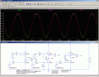
Comparison between three options:
1: Uncorrected
2: So-called "indirect feedback"
3: Plain-vanilla feedback
The same with a 5k load:
FET model is from Bob Cordell, so should be OK.
1: Uncorrected
2: So-called "indirect feedback"
3: Plain-vanilla feedback
Code:
Direct Newton iteration for .op point succeeded.
Fourier components of V(out1)
DC component:9.87571

Harmonic	Frequency	 Fourier 	Normalized	 Phase  	Normalized
 Number 	  [Hz]   	Component	 Component	[degree]	Phase [deg]
    1   	1.000e+03	4.995e+00	1.000e+00	  179.65°	    0.00°
    2   	2.000e+03	1.244e-01	2.491e-02	   87.15°	  -92.50°
    3   	3.000e+03	5.081e-03	1.017e-03	 -168.96°	 -348.61°
    4   	4.000e+03	2.287e-04	4.578e-05	 -159.24°	 -338.89°
    5   	5.000e+03	5.110e-05	1.023e-05	   81.33°	  -98.32°
    6   	6.000e+03	1.203e-05	2.408e-06	   -8.97°	 -188.62°
    7   	7.000e+03	2.937e-06	5.879e-07	 -101.94°	 -281.59°
    8   	8.000e+03	7.414e-07	1.484e-07	  165.18°	  -14.47°
    9   	9.000e+03	1.897e-07	3.799e-08	   71.36°	 -108.29°
Total Harmonic Distortion: 2.492889%


Fourier components of V(out2)
DC component:10.0331

Harmonic	Frequency	 Fourier 	Normalized	 Phase  	Normalized
 Number 	  [Hz]   	Component	 Component	[degree]	Phase [deg]
    1   	1.000e+03	4.990e+00	1.000e+00	  179.46°	    0.00°
    2   	2.000e+03	3.303e-02	6.618e-03	  -91.66°	 -271.12°
    3   	3.000e+03	1.022e-03	2.047e-04	 -111.52°	 -290.99°
    4   	4.000e+03	8.687e-05	1.741e-05	  -77.73°	 -257.19°
    5   	5.000e+03	4.033e-05	8.083e-06	   70.89°	 -108.57°
    6   	6.000e+03	1.276e-06	2.557e-07	  134.22°	  -45.24°
    7   	7.000e+03	1.788e-06	3.584e-07	 -103.22°	 -282.69°
    8   	8.000e+03	7.224e-08	1.448e-08	  -50.50°	 -229.96°
    9   	9.000e+03	8.027e-08	1.609e-08	   80.42°	  -99.04°
Total Harmonic Distortion: 0.662168%


Fourier components of V(out3)
DC component:9.99643

Harmonic	Frequency	 Fourier 	Normalized	 Phase  	Normalized
 Number 	  [Hz]   	Component	 Component	[degree]	Phase [deg]
    1   	1.000e+03	5.046e+00	1.000e+00	  179.35°	    0.00°
    2   	2.000e+03	6.467e-03	1.282e-03	  -29.18°	 -208.53°
    3   	3.000e+03	1.065e-03	2.110e-04	  -97.33°	 -276.68°
    4   	4.000e+03	2.058e-04	4.079e-05	  172.17°	   -7.18°
    5   	5.000e+03	4.402e-05	8.723e-06	   81.65°	  -97.69°
    6   	6.000e+03	7.585e-06	1.503e-06	  -18.23°	 -197.58°
    7   	7.000e+03	2.860e-06	5.668e-07	 -136.36°	 -315.71°
    8   	8.000e+03	1.677e-06	3.323e-07	  174.27°	   -5.07°
    9   	9.000e+03	1.060e-06	2.102e-07	  174.87°	   -4.47°
Total Harmonic Distortion: 0.129945%
The same with a 5k load:
Code:
Direct Newton iteration for .op point succeeded.
Fourier components of V(out1)
DC component:9.8999

Harmonic	Frequency	 Fourier 	Normalized	 Phase  	Normalized
 Number 	  [Hz]   	Component	 Component	[degree]	Phase [deg]
    1   	1.000e+03	3.690e+00	1.000e+00	  179.74°	    0.00°
    2   	2.000e+03	1.002e-01	2.715e-02	   88.28°	  -91.46°
    3   	3.000e+03	3.293e-03	8.925e-04	 -174.33°	 -354.07°
    4   	4.000e+03	8.040e-05	2.179e-05	 -131.64°	 -311.38°
    5   	5.000e+03	9.678e-06	2.623e-06	   78.29°	 -101.45°
    6   	6.000e+03	1.690e-06	4.581e-07	   -5.78°	 -185.52°
    7   	7.000e+03	2.679e-07	7.261e-08	  -95.12°	 -274.86°
    8   	8.000e+03	6.708e-08	1.818e-08	  153.44°	  -26.30°
    9   	9.000e+03	1.760e-08	4.770e-09	    7.13°	 -172.61°
Total Harmonic Distortion: 2.715995%


Fourier components of V(out2)
DC component:9.96358

Harmonic	Frequency	 Fourier 	Normalized	 Phase  	Normalized
 Number 	  [Hz]   	Component	 Component	[degree]	Phase [deg]
    1   	1.000e+03	3.662e+00	1.000e+00	  179.60°	    0.00°
    2   	2.000e+03	3.661e-02	9.997e-03	   88.56°	  -91.05°
    3   	3.000e+03	3.680e-03	1.005e-03	 -177.24°	 -356.84°
    4   	4.000e+03	1.991e-04	5.436e-05	  -96.55°	 -276.16°
    5   	5.000e+03	9.923e-06	2.710e-06	   27.74°	 -151.86°
    6   	6.000e+03	5.644e-07	1.541e-07	   16.66°	 -162.95°
    7   	7.000e+03	1.230e-07	3.358e-08	  -97.20°	 -276.81°
    8   	8.000e+03	3.749e-08	1.024e-08	  160.06°	  -19.54°
    9   	9.000e+03	1.989e-08	5.431e-09	  130.12°	  -49.49°
Total Harmonic Distortion: 1.004717%


Fourier components of V(out3)
DC component:9.9884

Harmonic	Frequency	 Fourier 	Normalized	 Phase  	Normalized
 Number 	  [Hz]   	Component	 Component	[degree]	Phase [deg]
    1   	1.000e+03	3.702e+00	1.000e+00	  179.51°	    0.00°
    2   	2.000e+03	7.936e-03	2.144e-03	   71.83°	 -107.69°
    3   	3.000e+03	4.374e-04	1.182e-04	 -134.20°	 -313.71°
    4   	4.000e+03	4.212e-05	1.138e-05	 -176.95°	 -356.47°
    5   	5.000e+03	7.767e-06	2.098e-06	   64.95°	 -114.57°
    6   	6.000e+03	2.806e-06	7.579e-07	   -3.78°	 -183.30°
    7   	7.000e+03	1.449e-06	3.914e-07	   -6.57°	 -186.08°
    8   	8.000e+03	1.278e-06	3.453e-07	    0.33°	 -179.18°
    9   	9.000e+03	1.177e-06	3.179e-07	    0.63°	 -178.88°
Total Harmonic Distortion: 0.214714%
FET model is from Bob Cordell, so should be OK.
Attachments
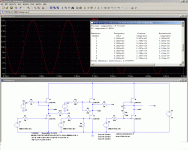
Interestingly, the distortion in #3 is caused by the large junction capacitances of the K170, and reducing the impedance level reduces the distortion further:
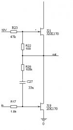
As in the example from MarcelvdG, the difference is that with "Indirect feedback" approach you have a high input impedance, but with "Plain-vanilla feedback" you have very low input impedance. I came up with this circuit for a particular reason: to make a single-stage low-gain voltage amplifier with good linearity and high input impedance.
Cheers
Alex
With those values, it isn't the Nikitin circuit anymore, it is regular feedback with a bit of make-up.If you compare two circuits: Applying negative feedback to the Nikitin circuit makes it even better, with a distortion less than 0.05%. But then you have a totally different amplifier as pointed out by Alex.
The resistance ratio is 4700:1, and if you make it ∞:1, it will make little difference.
it isn't the Nikitin circuit anymore, it is regular feedback
Yes it is. But you compared the Nikitin with your no3 circuit which has regular negative feedback. That was my point.
Interestingly, the distortion in #3 is caused by the large junction capacitances of the K170
Hi!
as usual we think THD
and forget about the harmonics distribution.
I think that harmonics plots from LTSpice up tp 10MHz will tell more
than THD%...
Yes I did.Yes it is. But you compared the Nikitin with your no3 circuit which has regular negative feedback. That was my point.
I did so with "pure" circuits, whereas you attempted to mix the two.
But the schemes are mutually exclusive: both set a defined voltage gain, determined by a resistance ratio.
If you implement them simultaneously, the overall gain will be lower, and the performances will be intermediate: worse than for pure feedback, but better than pure Nikitin.
Other compensation schemes like the X-quad leave the initial gain intact (it can increase it in fact), while giving a two orders of magnitude improvement in linearity, allowing the feedback and compensation to work in synergy, not concurrently.
Interesting facts. Aleph CS and SRPP are also in my opinion closely related.I find some analogy between this your approach and Nelson's Aleph current source. You deal with jFETs and modulation on the basis of output voltage, Nelson with MOSFETs and modulation taken from the output current.
I was playing several years with the Aleph current source, making modulation weaker or stronger, and removing it at all. Measurement-wise, modulation always improve THD. However, soundwise, the best result (most live-like sound) was without modulation at all (suppose, due to effects of PS, which provides variable output signal current in the case with modulation). However, I am sure, the variants with modulation will sound better, if one would attach a relevant shunt power supply to this stage. However, this can have sense for preliminary stages only, not for output stage of power amp.
For me, your approach to linearisation immediately rises a question of a dedicated shunt PS for this stage. It is attractive to add modulated load to this my jFET schematics
http://www.diyaudio.com/forums/solid-state/197493-jfet-amp-current-nfb.html
However, first I should find out an amp, that will sound better than this schematics, at low wattage applications. Subjectively, from direct comparisons with transistor and SE and PP tube amps, and from indirect comparisons (sound memories from listenings of best brands in Singapore) I do not have motivation for further modifications. Maybe they could be important for commercial purposes, if I would obliged to report better THD.
Concerning the listening tests with the Aleph CS (by a ZEN project with Aleph current source) I had found the same acoustical results as you.
Please let me know, in which commercial amplifiers this topology is in use - thank you.When I've designed this circuit in 2004 I had the same question and made some enquiries. The conclusion was that this is a case of what is called indirect feedback. Cheers Alex
Last edited:
Please let me know, in which commercial amplifiers this topology is in use - thank you.
So far only in the A.N.T. Audio Amber 3T Headphone amplifier. Hi-Fi World review is here:
www.ant-audio.co.uk/reviews/A.N.T. Audio Amber 3T.pdf
However it will be used in a new preamplifier design and a new headphone amplifier design that will be released early next year. Prototypes were shown at the UK Show in Whittlesbury this year.
Cheers
Alex
Thank you for this advices.So far only in the A.N.T. Audio Amber 3T Headphone amplifier. Hi-Fi World review is here:
www.ant-audio.co.uk/reviews/A.N.T. Audio Amber 3T.pdf
However it will be used in a new preamplifier design and a new headphone amplifier design that will be released early next year. Prototypes were shown at the UK Show in Whittlesbury this year. Cheers Alex
An "Off Topic" Question:
do you know details about CEC's LEF topology ? - go to
CEC HD53R
CEC HD53R Ver 8.0, newbie help
http://www.diyaudio.com/forums/solid-state/127182-lef-load-effect-free-amplifier-technology.html
http://www.diyaudio.com/forums/pass-labs/5808-cec-amp71.html
http://www.diyaudio.com/forums/solid-state/168185-how-does-lef-load-effect-free-amplifier-work.html
http://www.diyaudio.com/forums/soli...3300-amp5300r-lef-class-schematic-wanted.html
Thank you for this advices.
An "Off Topic" Question:
do you know details about CEC's LEF topology ? - go to
CEC HD53R
CEC HD53R Ver 8.0, newbie help
http://www.diyaudio.com/forums/solid-state/127182-lef-load-effect-free-amplifier-technology.html
http://www.diyaudio.com/forums/pass-labs/5808-cec-amp71.html
http://www.diyaudio.com/forums/solid-state/168185-how-does-lef-load-effect-free-amplifier-work.html
http://www.diyaudio.com/forums/soli...3300-amp5300r-lef-class-schematic-wanted.html
No, I have no knowledge on that one, sorry!
Cheers
Alex
Hi all,
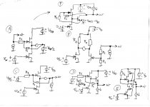
Some of the disadvantages of indirect feedback can be reduced by increasing the loop gain by putting an extra amplifier in the loop. I've been thinking about this and attached are all schemes I could come up with. All ideally have a gain of -(R1+R2)/R1, except version B which has a gain of +(R1+R2)/R1. I haven't drawn the resistors at the input, presumably Alex uses them to match distortion due to (capacitive) gate currents.
Some things you should know to be able to read the schematics:
-The word "uit" is Dutch for "out".
-The single circles with no line inside are nullators, network elements having no voltage across them and no current flowing through them. Basically this is an ideal model for the input stage of a high-gain amplifier in a feedback loop.
-The double circles are norators, network elements that can carry any current and can have any voltage across them. Basically this is an ideal model for the output stage of a high-gain amplifier in a feedback loop.
-Hence, a single circle and a double circle together model a high-gain amplifier.
Schematic A has a high-gain amplifier driving the load and the feedback network. The amplifier is connected such that it makes the drain-source voltages of both FET's equal to VDD/2, thereby eliminating errors due to finite FET voltage gain.
Schematic F is an implementation of A where the high-gain amplifier is a single transistor.
Schematic B is a non-inverting variant.
In schematic C I've swapped the norator and the voltage source compared to schematic A. As a result, you get the errors due to finite FET gain back, but the loop amplifier can be a simple voltage follower. This circuit is close to the original of Alex; use a wire as the voltage follower and you have the circuit of Alex back.
Schematic D is an implementation of schematic C using an emitter follower.
Schematic E is a variant of schematic D having the cascodes that Alex recommended in one of his posts. It also shows that the second voltage source can be disgarded when (R1+R2)/R1 times the VBE of the bipolar transistor is somewhere near half the supply voltage.
One disadvantage that cannot be eliminated is the fact that mismatch between the FET's results in distortion. A difference in pinch-off voltage only creates an offset, but differences in the shapes of the curves result in distortion no matter what.
Best regards,
Marcel
Attachments
Last edited:
- Status
- This old topic is closed. If you want to reopen this topic, contact a moderator using the "Report Post" button.
- Home
- Amplifiers
- Solid State
- Indirect feedback with FETs