It seems to be the hallmark of a good PCB layout to not have jumpers, or at least very few of them. For the DIY crowd just how frowned upon are they? IMHO a few jumpers should be fine, especially if it avoids really loony trace routing. I ask as my current rip-up and re-route looks like it may need a few links on the board.
I'm not entirely sold on the cancellation of the fields produced by the power supply traces, they occur at different times and therefore are not in exact opposition.
It's worth reading Doug Self's Audio Power Amplifier Design Handbook where he presents some example traces showing various distortion measurements, including this. This particular source of distortion (number 6), he calls induction distortion and says it 'is probably the most widespread cause of unnecessary distortion.'
With regard to its minimisation he says 'Minimise radiation from the supply rails by running the V+ and V- rails as close together as possible. Keep them away from the input stages of the amplifier, and the output connections; the best method is to bring the rails up to the output stage from one side, with the rest of the amplifier on the other side. Then run tracks from the output to power the rest of the amp; these carry no halfwave currents and should cause no problems'
It seems to be the hallmark of a good PCB layout to not have jumpers, or at least very few of them. For the DIY crowd just how frowned upon are they? IMHO a few jumpers should be fine, especially if it avoids really loony trace routing. I ask as my current rip-up and re-route looks like it may need a few links on the board.
Use jumpers as necessary, the important consideration is the performance, not what people think about them or frown upon. A large number of jumpers is sometimes indicative of a low effort having been made, but if you are satisfied that they result in a higher-performing layout, then use them as you see fit.
So, here's another iteration.
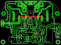
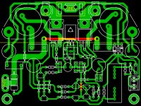
Does this represent progress? I think it does, though any layout is a compromise. Rail fusing will be on the PSU board and remainder of the output network on a remote board at the speaker output terminals. The speaker ground will be returned directly to the PSU. Any constructive comments welcome with respect to layout.
Thanks for the input thus far.
Attachments
Perfect, just where it should be............... Rail fusing will be on the PSU board ..............
I love your local HF decoupling !
Any room to fit in some MF decoupling? Try 100uF on each rail somewhere.
Add a pair of inverse parallel diodes across R3.
Last edited:
")
Hi Jason ,
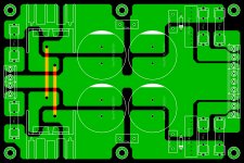
Layout based on your PCB , sorry if I'm not welcome in your thread.
Regards Alex.
Good to see you! You are very welcome to participate. I started this thread to help me learn about the finer points of PCB layout through community feedback. I only wish I was half as fast at a board iteration as you. I spend a great deal of time staring at the screen, visually routing and reorganizing before really doing anything.
Do you have any specific comments about my layout, good or bad?
Alex,
A couple observations regarding your layout, perhaps you could provide some feedback.
You provided two spades for ground connections, but they are physically connected via traces. What's the reason or rationale?
The outputs, drivers and VBE multiplier are intended to be attached to an L-bracket, the mounting holes in the upper corners probably don't need to be there, unless it is recommended to physically bolt the bracket to the PCB with dedicated hardware. Should there be dedicated fixing points or can the mounting screws for the devices be used exclusively?
Some of my earlier iterations included the output inductor since the space seemed to be available for it. Community feedback suggested it is best located at the output terminals so I moved mine off-board. Many of your layouts include the inductor in the PCB. Any specific thoughts on wether it should be on / off and why? I like the 'all-in-one' idea personally, but others seem to prefer a more modular approach with physical separation of certain blocks.
Thanks for providing some food for thought and an example from a more experienced perspective.
Perfect, just where it should be.
I love your local HF decoupling !
Any room to fit in some MF decoupling? Try 100uF on each rail somewhere.
Add a pair of inverse parallel diodes across R3.
Thanks Andrew. After seeing Alex's example I have a few ideas to incorporate into the next iteration.
Any thoughts on 'rail catching' diodes, reverse biased from output rail to power rails? Came to mind when you mentioned putting diodes across the 10 ohm ground isolation resistor for the audio grounds.
jkuetemann ,
What can I say , your board it's fine , I have learned a lot, myself from this thread . The skill comme by every layout , so we can practice all time we have , dedicated to prepare PCB's. I like PCB's compact , all in one ,so my PCB look like this attached below.
Regards Alex.
What can I say , your board it's fine , I have learned a lot, myself from this thread . The skill comme by every layout , so we can practice all time we have , dedicated to prepare PCB's. I like PCB's compact , all in one ,so my PCB look like this attached below.
Regards Alex.
Attachments
Last edited:
split power attachments as on Alex' is not the way to layout.
You disagree with power being delivered via the other side of the TO-3 flange? I wouldn't have thought it to have made much difference and eases the placement of MF decoupling, rail catching diodes and facilitates board testing prior to fitting the output transistors. I rather liked the approach. What is the issue? There are no long traces involved and essentially the power is still being delivered directly to the outputs.
Or did I miss something else in Alex's layout? It is fundamentally very similar to mine, but with his own signature flair.
I understand what you are suggesting now, not so much an issue on the PCB but rather the power delivery to the PCB. Fair enough. Like I said before this is an exercise in skill development.
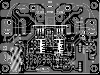
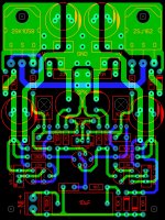
So, here's a few changes. MF rail decoupling, diodes across the audio ground isolation resistor, some rerouting of traces and a few components moved. Still haven't decided where the place catching diodes just yet.
Thanks for the active discussion so far folks, it might not be pretty but I think I'm beginning to see the light.
Attachments
The input fuses can't do much to improve safety.
]The high charge rates into the discharged capacitors require high value T rated fues.
These fuses then tolerate enormous overload currents.
Far better to close rate the transformer primary circuit fuse.
eg 200VA with 110/120Vac mains requires <=2A fuse to run the following 100W to 150W of maximum output power amplifier all day long at party volume levels.
I would experiment with T1.6A and T2A, to see just how low in fuse rating I could go, without incurring nuisance blowing.
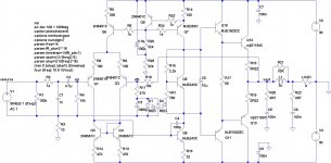
Power Supply for Audio Power Amplifier
Hi Jason,
I am basically doing a similar task as you are. I have designed a power amp using the LME49830 + LatFet, similar as was done by OPC (Owen). I managed to get a used transformer from a scraped Pioneer SX-1250 via eBay. I am merging two designs, the power supply section of the SX-1250 & the National Audio Power Amp Power Supply application note. I have done the Power Amp Recifier assembly & the PowerAmp assembly, so far and working on the attached PCB/schematic of the AC input assy. Still need to figure out the regulator for the LME49830, probably will just use a simple LM317/337, for that. Disregard the thin traces, as I just did a quick route last night, they will be beefed up with thick traces & copper pours. This gives me a chance to have people review what I am doing and get feedback as well. Hope that this is of some help to you. If you have any question, please ask.
Regards
Rick
Attachments
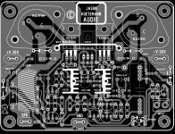
I know this thread has been left for some time, but I have been continuing to evolve and want to put a PCB layout up for comment. This is a VSSA variant and in no way related to prior examples I have posted on this thread before.
I have tried to keep loops tight and local. Since my current plan is to have a board house produce the board I have elected to make use of both sides of the board. This allows for the use of PTH and more convenient routing. Where a change of layer was desired I used a component lead location for the purpose. I have tried to allow for generous clearances and keep silkscreen neat and off the pads.
Any constructive comments welcome, tell me what you do or do not like about it and why. Thanks.
Attachments
- Home
- Amplifiers
- Solid State
- PCB Layout Process and Guidelines?