I'm currently in the process of creating a few PCBs using Sprint Layout and a few questions have come to mind. I'd like to get a few responses and points of view for PCB layout specifically for solid state design (which is why I posted here).
There are a few good nuggets of information scattered in various projects, particularly with respect to grounding and bypassing. I have been finding it difficult to get a high level overview of the subject with good generalizations.
Some of my most basic questions for those who are good at producing quality layouts:
1) What components to place first, where and why?
2) General workflow direction, from input to output, or from output to input?
3) What traces are laid out first, power and grounds or signal?
4) Choosing PCB size and shape, what are the primary factors in selecting PCB dimensions.
5) What components to place on the amplifier module and what should be on the PSU, such as fusing. If one places fuses in the PSU outputs is it still considered 'good form' to put a set on the amplifier PCB?
I welcome any advice and opinions pertaining to the above or otherwise that will help me down the right path when doing a design. Thanks.
Some of my most basic questions for those who are good at producing quality layouts:
1) What components to place first, where and why?
.
I usually start by staring hard and long at the schematic to get a feel for the signal flow and how to make it compact. Then change the schematic to make for a better geograpgy. Then decide on the PCB to be long and narrow (mostly) or narrow and wide (seldom)
Then I start layouting generally with the components in the middle and work my way towards input and output.
3) What traces are laid out first, power and grounds or signal?
.
I keep all supply lines to the top or bottom, kind of rails at the extremes and 'fingering in'to the parts to be supplied. Use local decoupling at each load point.
Ground should be as close to the signal circuits as possble. Use a ground plane if you can for signal ground only. Use only one point to connect the signal grounds to supply ground. Use star ground to connect the input- and output signal grounds together.
5) What components to place on the amplifier module and what should be on the PSU, such as fusing. If one places fuses in the PSU outputs is it still considered 'good form' to put a set on the amplifier PCB?.
Everything that does not necessarily need to be on the signal PCB should stay off of it! Just feed clean DC to it, and use local bypassing and/or regulation as needed. Fuses go on the supply board.
My 2 eurocents worth.
jan
This is the one I normally point people at - simple, common sense from a very experienced designer...l
http://www.alternatezone.com/electronics/files/PCBDesignTutorialRevA.pdf
Cheers
http://www.alternatezone.com/electronics/files/PCBDesignTutorialRevA.pdf
Cheers
Hi Jason,
I am not a professional layouter, but I like to do layouts and learned a lot of somebody, whose profession it is.
Let me give you 2 different layout examples for the same (nearly) amplifier, the FETZILLA.
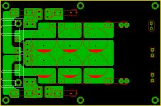
This layout has been done by Hugh Dean (I hope, Hugh doesn't mind showing his layout in this context):
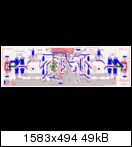
http://www.abload.de/img/fetzillapcb9usw.gif
This is how I did it:
http://www.abload.de/img/topviewhueb.jpg
Hugh has his "hand-writing" concerning layout, AlexMM has, I have, ...
(To read Hugh's and my name in the same sentence, ... !)
I am sure, there is no "best hand-writing".
If you do the layout carefully, if you try and keep the tracks as short as possible, if you adhere to some restrictions like running long tracks in parallel... : your own layout will do the job safely as well.
I will now try and answer your questions:
As I told you: I am a layout - amateur, and I still have to learn quite a lot.
Best regards - Rudi_Ratlos
I am not a professional layouter, but I like to do layouts and learned a lot of somebody, whose profession it is.
Let me give you 2 different layout examples for the same (nearly) amplifier, the FETZILLA.
This layout has been done by Hugh Dean (I hope, Hugh doesn't mind showing his layout in this context):

http://www.abload.de/img/fetzillapcb9usw.gif
This is how I did it:

http://www.abload.de/img/topviewhueb.jpg
Hugh has his "hand-writing" concerning layout, AlexMM has, I have, ...
(To read Hugh's and my name in the same sentence, ... !)
I am sure, there is no "best hand-writing".
If you do the layout carefully, if you try and keep the tracks as short as possible, if you adhere to some restrictions like running long tracks in parallel... : your own layout will do the job safely as well.
I will now try and answer your questions:
- I always start with the output-transistors on the top of the PCB. Positioning these transistors, the emitter resistors, the Zobel, the TEMPCO, ...
- I start from top to bottom and vice versa at the same time
- I start with the power lines, proceed with power GND and do the signal GND at last.
When I am done with the layout, I restart and optimize the Power GND (make it as "big" as possible). - Keep the tracks as short as possible, keep the PCB size as small as possible. The larger the PCB size, the more the PCB will cost!
- You should not have asked this. This is a question of faith! I have made a bad experience once putting rectifiers, power caps and AMP
on the same PCB. Hugh and others seem to have not made this experience.
In my next layout I will place the power caps on the AMP PCBs, but leave the rectifiers apart.
It is the power caps that store the energy for the output-transistors and the shorter the way to them is, the quicker the current can be forwarded.
As I told you: I am a layout - amateur, and I still have to learn quite a lot.
Best regards - Rudi_Ratlos
I usually start by staring hard and long at the schematic to get a feel for the signal flow and how to make it compact...
Then I start layouting generally with the components in the middle and work my way towards input and output.
I keep all supply lines to the top or bottom, kind of rails at the extremes and 'fingering in'to the parts to be supplied. Use local decoupling at each load point.
Ground should be as close to the signal circuits as possble. Use a ground plane if you can for signal ground only. Use only one point to connect the signal grounds to supply ground. Use star ground to connect the input- and output signal grounds together.
Everything that does not necessarily need to be on the signal PCB should stay off of it! Just feed clean DC to it, and use local bypassing and/or regulation as needed. Fuses go on the supply board.
There seems to be two schools of thought, One is a design from the inside out, the other outside in. I tend to be drawn to the latter, place the high current, PCB real-estate sucking components first, the rest fits where it fits.
This is the one I normally point people at - simple, common sense from a very experienced designer...l
http://www.alternatezone.com/electronics/files/PCBDesignTutorialRevA.pdf
Cheers
That looks like a good article on the subject I had not seen before, thanks.
snip...
If you do the layout carefully, if you try and keep the tracks as short as possible, if you adhere to some restrictions like running long tracks in parallel... : your own layout will do the job safely as well.
I will now try and answer your questions:
- I always start with the output-transistors on the top of the PCB. Positioning these transistors, the emitter resistors, the Zobel, the TEMPCO, ...
- I start from top to bottom and vice versa at the same time
- I start with the power lines, proceed with power GND and do the signal GND at last.
When I am done with the layout, I restart and optimize the Power GND (make it as "big" as possible).- Keep the tracks as short as possible, keep the PCB size as small as possible. The larger the PCB size, the more the PCB will cost!
- You should not have asked this. This is a question of faith! I have made a bad experience once putting rectifiers, power caps and AMP
on the same PCB. Hugh and others seem to have not made this experience.
In my next layout I will place the power caps on the AMP PCBs, but leave the rectifiers apart.
It is the power caps that store the energy for the output-transistors and the shorter the way to them is, the quicker the current can be forwarded.
As I told you: I am a layout - amateur, and I still have to learn quite a lot.
Best regards - Rudi_Ratlos
As for my last question, I was not really suggesting integrated PSUs, but rather wether or not things like fuse holders should be on the amplifier or not. I suppose it will depend on your PSU design, one PSU for multiple amplifiers or dedicated PSUs for each, would determine if separate fusing is desirable or not. Guess I answered my own question on that point.
Some food for thought so far, thanks folks. I have a some partially done, I'll post back what I have done for feedback when they are closer to complete.
I believe in starting with the case, then design the boards to fit the case... especialy important with smaller and portable designs. In power amps, heatsinks are often needed as part of the case design. Each heatsink would have an optimal spaceing to give attached output devices an equal share of the cooling capacity. So once you know how big the sink is and where the outputs should optimaly go, it gets easier to add the intermediary stages.
Where posible group parts into their functional properties, like CSS etc. this makes servicing easier to someone not familiar with the boards.
Some designers like our own Graham Maynard are realy good at drawing schematics which can be virtualy duplicated in terms of physical layout, without moving parts around.
Towards the input side, you want to keep traces short and take note of things like thermal tracking in LTP etc...
As for fuses, yes it realy depends on design.
I was trying to figure out why my mini aleph rails were consistantly lower than what simulating would suggest (which is an issue on an amp like that with limited voltage swing ability to start with), becasue I hastily assempled the PSU slapping two PSU pcbs in series (each which had onboard fuses with an esr of about 160m Ohm). Sadly the fuses are not in the ideal places to create a CRC effect with, and if one were to add them there they would not be in an ideal place to disrupt power fast after tripping, as there would then be a capacitor bank still between them and the amp.
I think good practice is to protect components in order of what they cost to replace, starting with the most expensive, your house, so fuse before transformer is of prima importance. Fuses after transformer has diffirent things to concider and sometimes are not usefull at all for protecting against anything but fire hazard. Download some fuse datasheets and become familiar with their real operating behaviours.
A fuse is not a switch which breaks when it reaches a set threshold. It is more like the SOA knee of a transistor which needs to be exceeded by one or other mechanism, either less power over more time, or more power over less, time, but time is always a factor.
1: Any component that requires special mounting like your power devices to a heatsink go on first.
2: input to output or vice versa? I think it's personal choice though I tend to go input to output.
3: I lay on power / ground initially because it's best if it's minimally disrupted and it HAS to be there. Resistors make fine jumpers over power traces. The video boards I did were mostly 4 layer with a solid ground plane. The other middle layer was primarily power routes or if needed, signal routes that will never need to be altered. I've not tried 4 layer for audio but I'd expect it to be very good if not better.
4: I try for rectangular boards with as few routes as possible as they cost less. 'Routes' are special cuts / cutouts for oddly shaped boards. Size often has mechanical requirements for chassis or card cages. Or, leave enough space around power devices so it doesn't 'cook'.
5: Any devices that cause a lot of mechanical stress are better chassis mounted if possible.
G²
Member
Joined 2009
Paid Member
This is a question of faith! I have made a bad experience once putting rectifiers, power caps and AMP on the same PCB. Hugh and others seem to have not made this experience.
In my next layout I will place the power caps on the AMP PCBs, but leave the rectifiers apart.
It is the power caps that store the energy for the output-transistors and the shorter the way to them is, the quicker the current can be forwarded.Best regards - Rudi_Ratlos
In terms of the psu I worry about two things.
First, the very high current surge/spikes that naturally flow in the transformer secondary - through rectifier diodes - through first barrage of filter caps. I don't want any of this on my pcb unless it's out at the edges like Hugh does it. If I can't afford the space to do it his way, then I want it off the pcb.
Either way, I want the current loop area that these large current charging spikes flow around to be as small as possible so they don't couple and radiate into my small signal circuits. This means I want the secondary of the transformer - recifiers - caps to be physically very close to each other with all wiring twisted pairs. The twisted pairs should carry counter-flowing current so that their magnetic fields overlap and cancel out as much as possible.
So if you put any part of the psu on the amp board, you want the rest of the psu mounted very close to the amp board itself. You also want to ensure you have thick & wide traces on your pcb where these large spike currents are flowing.
The second thing I worry about is high frequency noise generated by the rectifier diodes 'switching' on and off. I follow Hugh's recommendation and use soft recovery diodes (that's not the same thing as slow recovery). And if possible, in-line chokes. You don't want these chokes anywhere too close to your amplifier as they do leak magnetic flux. Just like output inductors - you don't want these anywhere close to each other or your small signal circuits either.
And a small afterthought - power supply filter caps - electrolytic caps don't like heat - keeping them away from the hot output stage will lengthen their lifetime. It's an exponential relationship - a drop in temperature has a significant benefit.
Anyhow, I'm not in a position to talk much from experience, these are just the guidelines I give to myself.
Last edited:
Member
Joined 2009
Paid Member
In terms of pcb design:
I haven't made many so again I'm not an expert in any fashion. But here are some of my thoughts:
a) I like to keep the main power rails close together so that countervailing current flows are adjacent - minimizes area of loop for magnetic coupling. I also like to keep them short and fat and away from the small signal parts of the circuit. Most everyone else likes to separate the power rails around opposite edges of the pcb - the opposite to my philosophy.
b) Think about where the big currents flow through the load. I find that in most cases I don't have to worry about large currents flowing through the GND on the amplifier pcb - those big currents all happen off board. I place my star gnd at the speaker gnd connectors. On my amplifier pcb the big current flows occur only in the + and - rails.
c) I haven't used a ground plane but may try it in my next design. I do know that a ground plane is a complex animal - it is NOT an equipotential once you move away from dc currents. If you place a ground plane on the one side of your pcb and then run signal traces on the other side, the return currents for these signals will tend to follow the path of the signal traces as they return through the ground plane. You need to consider a ground plane as behaving like a mirror image of the signal traces with all the consequences of cross-talk. The higher the frequency the more this is important. With no ground plane consider carefully where return current flow back to the gnd connector on the pcb - shared ground traces are OK where currents are small, but any larger currents warrant their own trace.
d) Place the 'must have' parts first - usually you have no choice about the power devices. You may also want to place trimmers and connectors in places where they can be accessed. You may need mounting holes.
e) I then partition the board into areas - high current power, low current signal, feedback paths etc. and then layout into these areas. I am careful near any sensitive high impedance points such as the feedback node and input (i.e. the LTP on amplifiers that use them) as these are very prone to capacitive coupling of unwanted signals - you can end up with an oscillator instead of an amplifier this way.
f) If the layout is not pleasing to my eye then I will change it. Don't ask me why, but it seems an important part of the process for me.
p.s. use large pads for through-hole parts, easier to work with and less likely to lift up when you have to replace the part in question because you blew it up !
Last edited:
Hooray - a voice of reason!a) I like to keep the main power rails close together so that countervailing current flows are adjacent - minimizes area of loop for magnetic coupling.
")
I'd add that in a class AB amp, the same or greater care should be taken to minimize the loop area for the half wave rectified output stage currents, but only if you want to achieve very low distortion.
A lot of folks like to "spice up" their amps with some pleasant sounding distortion, though. For example the two layouts posted earlier by Rudi are excellent examples of how to get the maximum possible even-order distortion from magnetic coupling. The second one also has the feedback take-off point offset to get more distortion another way.
Some good direction thus far, thanks much. This seems as much or more an art than a science. The last time I did an audio PCB it was bone with flm, tramsfers and pen!
Any pointers on using the toner transfer method for PCB creation? I have always used photographic thechniques but might like to try what seems a simpler method for one or two boards. Recommendations?
Any pointers on using the toner transfer method for PCB creation? I have always used photographic thechniques but might like to try what seems a simpler method for one or two boards. Recommendations?
The magnetic fields won't cancel but there's a choice of whether they sum to a fairly accurate replica of the audio signal, or a full wave rectified version thereof i.e 100% distortion.The problem with this approach is that the two currents, pos and neg, do not occur at the same time and thus do not cancel.
PCBs are designed in the real world and are subject to constraints other than those affecting absolute performance.
When laying out a PCB the first considerations are: what are the dimensions of the available space, does the physical design call for a particular arrangement of connectors, and are there any thermal requirements such as heat-sinking.
In a PCI soundcard, for example, the PCI connector and the location of the audio I/O are pretty much a given.
If there are no such considerations, then the design can proceed purely on the basis of performance, but it is a rare circumstance in which absolute performance is the only criterion. Even amateur constructions generally require a housing of some description, and the PCB design needs must take this into account. The volume knob is frequently the largest control and often centrally placed. A symmetrical, or semi-symmetrical front-panel layout is often chosen in deference to visual balance.
Thus the final design may require iteration and compromise. Physical layout must, in some instances, give way to electrical or thermal considerations. Thru-hole components give way to SMT where double-sided boards are mandated by a paucity of real estate (or by improved decoupling). A thru-hole board will never achieve the low strays and decreased grounding-loop areas of which SMDs are capable.
Modern designs frequently call for power connectors, I/O jacks, potentiometers, displays, transistors with heat-sinks and even tubes and larger transformers to be directly mounted on the board. CAD software makes this more straightforward to achieve now than it was in the past. As designers gain in experience they will naturally wish to incorporate such features as exemplify both good ergonomics and good performance. A sophisticated design, well thought through, will frequently require less effort in construction than one assembled on an ad-hoc basis from a heterogeneous collection of PCBs of arbitrary dimensions.
Even where connectors and other components comprising the user interface are panel-mounted consideration needs to be given to exactly how the connections between these components and the board will be made.
Layouts which work for commercial designs are likely to work for amateur ones, so mimicking existing devices is not the worst strategy.
Godfrey,
I was interested in your comment that I designed the FetZilla board to maximise even order distortion.
I'm not familiar with these techniques, would you like to explain precisely what you mean here?
We'll leave the argument about summing half wave current waveforms for now......
Cheers,
Hugh
I was interested in your comment that I designed the FetZilla board to maximise even order distortion.
I'm not familiar with these techniques, would you like to explain precisely what you mean here?
We'll leave the argument about summing half wave current waveforms for now......
Cheers,
Hugh
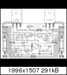
Partial PSU
Here's the start of my PSU. It will have boosted rails for IPS and VAS and will use two dual secondary transformers, 20V+10V, no centre taps. Will try to fit a capacitance multiplier for the boosted rails if space allows (still have to lay down rectifier, filter and other components for the boosted rails yet, obviously).
Comments and constructive criticism welcome.
Attachments
- Home
- Amplifiers
- Solid State
- PCB Layout Process and Guidelines?