any comments, does it fare anywhere near the acceptability criteria?
Hi Prasi,
Here are my comments:
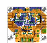
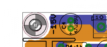
1) The two film capacitors at the output (C9/C10) are not needed, IMO. They are too far from the load and they are too far from the regs to do anything useful. But these has already been mentioned if I remember right.
2) The input terminal even if designed for CT transformer may be better with two CT pads to accommodate for dual secondary transformers. It is not always easy to squeeze two transformer leads into one terminal hole.
3) You can make a complete CT/GND pour around the input connector pins which cost nothing but can potentially reduce radiated ripple noise.
4) Big filter caps touching potentially hot heat sinks may significantly shorten capacitors life. I would make some clearance distance of at least a couple of millimeters there.
5) Traces on top layer under the heatsinks (made of conducting metal) are a potential problem if inexperienced diyer solders heatsinks sitting flat on the PCB. Relying on solder resist alone to insulate the heatsink from the traces is not a good idea. So some sort of spacers are needed to lift the heatsinks above the PCB which makes things complicated.
6) It would be easier to follow your PCB design if you would choose color scheme with higher contrast for visualization and with different color for exposed solder pads especially for SMD components, IMO.
Regards,
Oleg
Much better now and much easier to follow!
You can further improve the design by moving the mount holes at the power entry side a bit down to the board's edge and moving filter caps C1/C2 further apart, away from the input connectors. The CT/GND routing around negative pin of C1 and area with "many vias" south of 7815 reg can be further improved by simply connecting these two parts together on the same layer. There are no obstacles for doing it.
You can further improve the design by moving the mount holes at the power entry side a bit down to the board's edge and moving filter caps C1/C2 further apart, away from the input connectors. The CT/GND routing around negative pin of C1 and area with "many vias" south of 7815 reg can be further improved by simply connecting these two parts together on the same layer. There are no obstacles for doing it.
One more thing. Heatsink mounting holes need a bit more clearance around to prevent screw thread cutting into copper and thus shorting it. Also the use of insulating washers is necessary in current state since there are traces around the heatsinks' mounting holes on the bottom layer.
In manufacturing, usually the case was designed first and then the PCB. The size of PCB and maximum height at PCB area is fix, can not be change. So, PCB design is always compromise.
But in DIY, we free to set the size of PCB and the height of components.
Yes Bimo, agree completely.
very true for commercial production.
In diy people can customise for anything thats available.
e.g. just assembled a cabinet yesterday for a pre-amp/ small amplifier. I wanted it to do the duty of almost a universal case for pre and HPA / small amp.
Thats why many RCA holes (so as to fit a i/p selector) + it also has headphone jack hole, volume pot and speaker binding post.
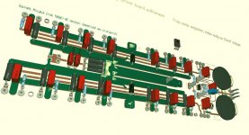
heat sinks can be mounted externally. Its from a production company here in India.
Attachments
One more thing. Heatsink mounting holes need a bit more clearance around to prevent screw thread cutting into copper and thus shorting it. Also the use of insulating washers is necessary in current state since there are traces around the heatsinks' mounting holes on the bottom layer.
the thick black line near the copper around the mtg hole is silk. the thin line inside is the actual hole on dim layer. so there is no issue.
In design yes, I agree, in production by cheap manufacturer the hole center position can be off by as much as 0.3~0.5 mm. So a bit extra clearance would never heart. Keep in mind that non-plated through holes are done after the circuit is ready and the registration of hole centers is not perfect in this stage. This is at least what I see on my PCBs.
Hole diameter 3.2mm non metal: 4mm in X/Y from edge of the board outline. You can define M3 washer PCB symbol only and M3 screw PCB symbol only (no SCH symbol needed), helps a lot for placing, routing (works as keep area) or modeling.
Colours:
- black souled background
- hell red for electrical bottom
- meadow green for top electrical
Like oblong pads for soldering, more vias for more copper and a lot more...
With permission, my 2 cents.
JP
Colours:
- black souled background
- hell red for electrical bottom
- meadow green for top electrical
Like oblong pads for soldering, more vias for more copper and a lot more...
With permission, my 2 cents.
JP
Hole diameter 3.2mm non metal: 4mm in X/Y from edge of the board outline. You can define M3 washer PCB symbol only and M3 screw PCB symbol only (no SCH symbol needed), helps a lot for placing, routing (works as keep area) or modeling.
Colours:
- black souled background
- hell red for electrical bottom
- meadow green for top electrical
Like oblong pads for soldering, more vias for more copper and a lot more...
With permission, my 2 cents.
JP
thats what my design uses, 3.2 mm hole and the rest around the hole is a symbol for washer on silk. like attached. apart from the silk, I keep a 'keepout' of about 1.5mm around the washer silk outline. see attached.
sometimes I prefer to keep 5 mm distance from edge, or depending upon user requirement of hole spacing. especially for very BIG and / or heavy component, 4mm may place too much stress in the corners.
but these things are mechanical considerations that will depend lot on application and will get corrected in routing revisions (I generally have 3-5 revisions for diy, for sponsored, it may go as high as 10-15).
mainly i was looking for comments on 'electrical' layout.
Attachments
I am getting the feeling that my german friends think I am beginner in designing. I have come a long way from 2014-15. all of my diy amp designs never failed to work as evident in many of the threads here like simple apex designs, some personally built ESP and other's designs, some new (only simulated designs) , many pre amps, head amps, class-A amps to much more complex designs.
in a way eagle has been a lot of help.
never had a mechanical/electrical layout related problem (some package/ component library pin out issues, yes). recent example is a Apex Supergain clone, I do not know if the particular ckt was tested before, but I was the first one here to lay it out (single sided mono, single stereo and double sided mono) and go on to test it and guess what?, it works perfectly. there are many such examples here, another notable one would be FX-100 design which was modified by me for 3-pair o/p, when tested works perfect.
In design yes, I agree, in production by cheap manufacturer the hole center position can be off by as much as 0.3~0.5 mm. So a bit extra clearance would never heart. Keep in mind that non-plated through holes are done after the circuit is ready and the registration of hole centers is not perfect in this stage. This is at least what I see on my PCBs.
have a look here, Printed Circuit Board Design Tolerances | Advanced Circuits
If you want to build something now-a-days leave it for the Chinese..
 they are cheap to manufacture and give better tolerances.
OK!
First connect heatsinks on ground, I don´t like potential free metal, I´ve a lot more ground material, TO220 isolated mounting.
Rectifier diode as close as possible on the AC input connector.
Post your schematics again.
Post EAGLE snapshot before Rastnest (colours as mentionned).
Thanks.
JP
First connect heatsinks on ground, I don´t like potential free metal, I´ve a lot more ground material, TO220 isolated mounting.
Rectifier diode as close as possible on the AC input connector.
Post your schematics again.
Post EAGLE snapshot before Rastnest (colours as mentionned).
Thanks.
JP
I´m not thinking that you´re beginner then you´re loving your work, that´s really important. Good layouts could be compared to a sort of modern art. My opinion.
What do you think about layouting together perhaps the coming Pass ACA-2?
JP
I am game to any layout related stuff!
In hindi language we have a proverb " Neki aur pooch pooch?" meaning "A good deed needs no permission."
regards
Prasi
I usually manufactured my prototype by cheapest one and got like 3mill max of error. 0.3~0.5mm must be diy-ed by your pcb seller, not manufactured by pcb manufacturer.In design yes, I agree, in production by cheap manufacturer the hole center position can be off by as much as 0.3~0.5 mm. So a bit extra clearance would never heart. Keep in mind that non-plated through holes are done after the circuit is ready and the registration of hole centers is not perfect in this stage. This is at least what I see on my PCBs.
Hello,
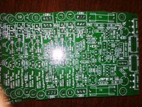
I'm currently designing the PCB board for the output + driver stage of a class Ab amplifier, rated 160Wrms/8R and +- 620Wrms into 2 ohms. Output stage will consist out of 7 pair 2SC1645/2SA2223 BJT's.
The PCB board will me made using 2oz copper thickness (70µm).
Now I'm wondering, would it be a good idea to mirror all the power traces to both sides of the board?
Any advice or confirmation would be nice.
Kind regards
Attachments
would it be a good idea to mirror all the power traces to both sides of the board?
Yes, but be sure to use thermal reliefs for soldering.
Last edited:
You sometimes can't afford thermal relief for high current paths, they become PCB fuses!
Then you'll need one of these.
Industrial Grade Heavy-Duty 550 Watt Soldering Iron with Stand and No Tip
- Home
- Amplifiers
- Solid State
- PCB Layout Process and Guidelines?