Yes, but be sure to use thermal reliefs for soldering.
Ok, after some googling I understand the purpose of this.
Never had problems with soldering 2oz PCB's with vias and copper on both sides of the pcb.
I'm using a Weller WS81 soldering station, not very special at all.
I was doubting about the loops which are created between the copper on one side of the board, the multiple vias and copper on the other side??
Any thoughts?
I was doubting about the loops which are created between the copper on one side
of the board, the multiple vias and copper on the other side??
Can you post a pdf of the board?
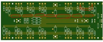
Offcourse, here it is.
Red: bottom copper
Blue: top copper
At this moment the blue traces are a mirrored image of the bottom traces.
This means in for example the power rail traces have 7 vias (for the collector connections) which connect bottom and top copper with each other.
My concern is that this will create loops which can pick up not wanted signal, or am I a bit to paranoid?
Attachments
Last edited:
It won’t be a problem. A technique that’s commonly used to increase power handling is to stitch the top and bottom layers with lots of vias in a grid. It’s expensive if your process charges for holes, but most don’t these days.
Alternatively put a gap in the solder mask along the trace, then run a bead of solder along the trace. Done properly you can get really high current capacity in small spaces.
Look at commercial SMPS PCBs. They use all the methods to get lots of current.
Alternatively put a gap in the solder mask along the trace, then run a bead of solder along the trace. Done properly you can get really high current capacity in small spaces.
Look at commercial SMPS PCBs. They use all the methods to get lots of current.
Well solder has a significantly lower conductivity than copper, so tack soldering a thick copper wire along the bare board is much more reliable (and calculable) way to lower resistance in critical areas as you need about one tenth the amount of extra metal and you won't get hot-spots due to variations.
You used to be able to easily get copper busbar strips with through-hole pins every 0.5" or so which was a great way to increase current handling, hard to find these days I think, but I did turn up this: E-FAB Bus Bars Copper Busbars & PCB Stiffeners | Photo Etching, Photo Chemical Machining & Micro Milling
You used to be able to easily get copper busbar strips with through-hole pins every 0.5" or so which was a great way to increase current handling, hard to find these days I think, but I did turn up this: E-FAB Bus Bars Copper Busbars & PCB Stiffeners | Photo Etching, Photo Chemical Machining & Micro Milling
I do an automatic auto-place function to place all components.
Then realise everything is in the wrong place so start again with what comes out of the schematic to pcb converter.
I hand place all components as close to other connected components as possible.
Once all is placed I do a "swap autoplace" function to get net as short as possible.
I make sure if there is a power supply on the pcb that it is star grounded so as not to interfere with low level audio signals.
Any input audio is kept short and where possible surrounded by ground plane.
I then start routing tracks, my software takes the shortest tracks first and routes them.
Once everything is routed I go back in and improve where possible.
Then I do an integrity check to make sure the schematic still matches the pcb.
I also do a clearance check then a continuity check.
I also make sure there is no vias under component references so the yare easily readable.
and add please a lot of vias to connect the planes together...
JP
Hi JP,
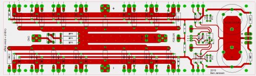
The small brown stars are ment to be vias with a diameter of 0.6.
What do you think, is this sufficiënt?
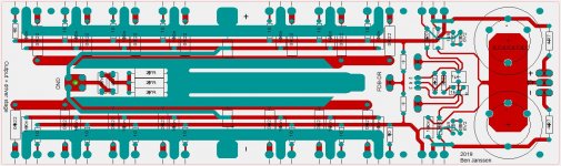
1e picture= top copper showed
2nd picture= top copper hided, vias locations are visible
Kind regards
Attachments
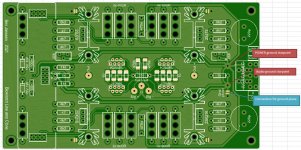
Ground plane - single connection to audio ground star point
Hello,
As I don't have much experience regarding ground planes, I would like to ask opinions or best practices on this matter.
I read both positive and negative opinions about ground planes.
What have I drawn?
1. Starpoint for power ground traces
2. Starpoint for audio ground traces.
Both audio and power startpoint are connected with a single trace.
3. A connection to be made with solder to connect the copper plane to the audio ground start point.
Is this any good? Will it give me more trouble with picking up noise.....
Kind regards
Attachments
The main thing is to avoid large changing currents modulating other signals due to resistance in pcb tracks.
This suggests star grounding is best way to go.
Certainly star grounding power and audio signal grounds is very good practice.
I designed a USB mixer many years ago and just laid out the pcb without any thought.
What I got back had 1VRMS of hum on the output !
What had happened was charging impulses into smoothing caps was modulating the ground line and injecting noise into audio circuit which was being amplified.
I reworked the pcb keeping audio ground and power supply ground separate and only joining them once at pcb connector for power. This time I had neglible hum.
- Home
- Amplifiers
- Solid State
- PCB Layout Process and Guidelines?