Hi Guys
Op-amp internal circuits and modern power amp schematics are pretty much identical. The difference is in the die area for each BJT.
Similarly, an op-amp driving an EF stage is commonly used as a line driver or headphone output, with TO-92 devices for the output. Change those to TO-220s, TO-3Ps, etc and you have current capability to drive a speaker.
In the buffered opamp circuit, there is typoically just an R from one side of the bias circuit to the supply. It is best to split this and bootstrap it for maximum head room. The current from this R goes through the opamp output.
A common error in such circuits is leaving out a small compensation cap around the opamp - typically 10s of pF - and a small series R between the opamp output and buffer - 10-100R.
Also, why do you want to amplify DC voltage? Best to incorporate a cap in the shunt portion of the feedback loop - should be 470uF or higher for low low-f THD.
Another also, why do you want to have scratchy pot noise? best to capacitively couple from the input level control to the opamp so the bias current of the latter does not flow through the pot wiper.
In the zeal to reduce parts count, most people over-simplify the circuit to the point of serious performance degradation. In a compound amplifier as you are discussing, there are certain parts that are necessary to assure stability unless you are going to extensively test components. Very good performance is possible with this arrangement.
Fitting in with the cheapo goal, a dual opamp would cover two channels, since presumably you want stereo.
The bootstrapped opamp supply trick is much older than LT, as national Semiconductor showed it in their 1980 Linear app book - likely predates even that.
Have fun
Kevin O'Connor
Who can upload this article?Thank you for this information.
A similar topology I have found in the magazine "Audio Amateur" 3/96 (THREE: 1996), start from page 22:
"10 Watt Class-A" by Dick Crawford.
Equipped with a dual OP-Amp "LT1124", one pair MOSFET IRFP150/RFH25P08 and an active bias part. Actually not exact matched for this topic, but through the great similarity in the circuit topology I mentioned here.
Perhaps one of the member can scan and upload this article.
Some ClassAB ensure more correct output biasing without the need for a Vbe multiplier.
Diode biasing and resistor biasing are both valid forms of output bias control.
In older push pull class AB power amplifiers there are to find in most cases diodes like that one from
http://www.ic72.com/pdf_file/z/179610.pdf
together with a variable resistor instead a Vbe multiplier.
But I don't understand why this is an advantage. Which benefit concerning the stability of the output biasing is here to expect? Are there existing investigations ?
Maybe I posted a message about my pure Class B amplifier circuit on this forum before:
A Pure Class B Audio Amplifier
You can easily alter it for much higher output using Darlington output transistor pairs and 3 diodes in series rather than one. You may need to experiment with the value of R3 to get the voltage at the emitters of Q3 and Q4 approximately to half the supply voltage.
A Pure Class B Audio Amplifier
You can easily alter it for much higher output using Darlington output transistor pairs and 3 diodes in series rather than one. You may need to experiment with the value of R3 to get the voltage at the emitters of Q3 and Q4 approximately to half the supply voltage.
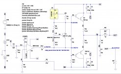
Here is the latest version of the circuit. A couple of resistors has been added around the Vbe pot to make the range of adjustment smaller and setting up easier. There is now a resistor on the output of the opamp, as suggested by Struth.
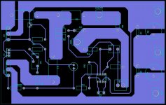
To take the concept from idea to reality, I have laid out a PC board. It is single-sided to simplify construction. There is still one zero ohm resistor where I could not quite figure things out.
A new version with a diode string replacing theVbe multiplier is on the drawing board. I am also thinking of adding short circuit protection in the form of a VI limiter. Putting it in detracts from the design goal of having a low component count, but is it worth the risk? The circuit is good enough for something like an active speaker, but in the real world bad stuff happens.
Attachments
Member
Joined 2009
Paid Member
It's usual to include a capacitor in series with R1, something around 47uF should be fine. The idea is that the feedback network will divide the output signal for music signals so that feedback is less than 100%, but for d.c. it will ensure 100% feedback. This ensures you have gain at a.c. but no gain at d.c. so that the d.c. offset at the output is more stable. It's usually necessary to employ a dc-servo circuit or a series output capacitor if you don't do this.
Another extra you could add, is a RC filter at the input, a 1k resistor after C4 and a 200p to 300p cap to signal ground - this will remove r.f. trying to sneak in.
R7 needs to be rated at 1W to 2W so you'll want to size this part on the pcb appropriately.
Perhaps you could make better use of the board space by increasing the footprint of the power supply rail capacitors. Heck, you might have space to include the power supply altogether, add the rectifier diodes. Then all you need to do is wire up the transformer !
Last edited:
After some more analysis, it turns out that replacing the NE5534 opamp with an OPA552 improves this design immensely. The biggest problem was the limited output power caused by the +21V supply. The power output capabilities of the TIP142/TIP147 are largely wasted. With a +30V supply allowed by the OPA552 power output goes up from 15W into 8 ohm ime to 40W. As a bonus, the distortion figures are down as well. THD is 0.0012% at 1kHz and 0.014% at 20kHz. That is if the SPICE model for the OPA552 is accurate. Time to etch boards and melt solder!
Attachments
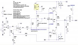
After some more analysis, it turns out that replacing the NE5534 opamp with an OPA552 improves this design immensely. The biggest problem was the limited output power caused by the +21V supply. The power output capabilities of the TIP142/TIP147 are largely wasted. With a +30V supply allowed by the OPA552 power output goes up from 15W into 8 ohm ime to 40W. As a bonus, the distortion figures are down as well. THD is 0.0012% at 1kHz and 0.014% at 20kHz. That is if the SPICE model for the OPA552 is accurate. Time to etch boards and melt solder!
One more case where simulation gets the better of you! Can the LM334 actually withstand the full voltage swing at the bases of the output darlingtons?
Also a little note on the previous NE5534 design - also usable to most such designs with older OPamps. They are made with a non-complementary process so making complementary transistors is quite difficult. Usually the output stage us then made a quasi-complementary design but the driver transistor for the negative rail is a lateral PNP, which is vastly inferior in performance to the remaining NPN parts in the OPamp.
In your design the OPamp is essentially forced to work in class A, since it has to sink more current than the output darlingtons ever need at their bases (the driving current as a rule must be only a small fraction of the base currents of the darlingtons, for the stage to operate with little distortion. In this design there is no VAS but rather a low impedance driver - the OPamp - so the criteria are somewhat relaxed, still it's the current source that must source all the current to the darlington base at maximum + swing, hence the current the OPamp has to sink is at least zero at positive clipping and increases as the output goes to -V).
The recurring problem in all these designs is the knee-jerk reflex to put the current source in the positive rail, when it is actually better re OPamp performance, to put it in the negative rail - the OPamp output then degenerates to a simple follower with very high bandwidth and negligible distortion at the required currents, the bottom half of it's output stage containing the low performance lateral PNP is completely turned off or runs at constant idle current.
Also, in a minimum part design I'd go with a bootstrap 'current source', also the VAS needs a capacitor in parallel. Unlike a regular amp with a VAS, where bootstrapping can be a problem since it relies on the output stage being a perfect follower (and it's not) and having no crossover distortion (and it does), this design has a low impedance drive from the OPamp, hence imperfections n the behavior of the bootstrap 'current source' have little influence to the OPamp output signal, unlike a classic VAS design where they directly translate into wrinkles in the VAS transfer function. Two resistors, a cap (albeit electrolitic) and perhaps a clamp diode to +V are cheaper than a LM334 with it's associated components, even though they might take a bit more space. And - it's easy to make them work with swings over 35V.
On another note, using lateral MOSFETs or even vertical MOSFETs will not get you too far, especially in the former case. A follower with a lateral MOSFET has gain significantly lower than 1 at currents of interest. It takes a Vgs of about 7-10V to drive a lateral to the full 7A of current. Hence, with a 22V power supply, you would be lucky to get 15V peak out of the amp, accounting for all the losses. On the up side, the biasing is very simple.
With vertical FETs it's going to be a problem unless low treshold FETs are used, this time not because of the follower gain but because of the high treshold voltage of the FETs (usually 3-4V), so again you are lucky to get 15V peak output.
There are however things you could look into.
1) The 'inverted' QSC/Hafler transnova topology is one, it does require separate power supplies for each channel. Using this topology and lateral FETs one can build a very capable amplifier, the high current capability of the NE5534 can drive a pair of laterals very well. However, keep in mind that the output transistors provide gain in this topology so additional care is needed to insure stable operation (compensation). Lateral MOSFETs are especially interesting in this configuration because they have the source terminal on the case, and in this cinfiguration both sources are connected to ground, hence no insulators necessary between transistors and heatsink!
2) A bridge topology. One could simply use a NE5532 here to get phase inversion from a single IC package. A particulairly interesting species of bridge is the CSPP, also known as Circlotron. Although this topology can be a bit tricky with power supplies (in theory, 2 independent ones are needed for each output stage, and one extra dual for the front end), it inherently offers a gain of 2, so the output swing immediately doubles in comparison to a follower topolog. It uses same polarity output devices, yet it's inherently completely symmetrical, and unlike the QSC/Hafler, very easy to compensate (in most cases, no extra compensation is required). A The place to look for ideas on how to drive a circlotron output stage using a dual OPamp, google the legendary J. Bongiorno's SUMO 'The 9' power amplifier. The same front end can also drive a classic bridge output stage.
Last edited:
One more case where simulation gets the better of you! Can the LM334 actually withstand the full voltage swing at the bases of the output darlingtons?
Thanks for the detailed reply and for pointing this out. A little voice at the back of my head told me to look into this late the other night when I was not near my PC, but I never got round to it.

LTspice shows a swing of 53V across V+ and V- while the datasheet specifies 40V. The high-voltage version of this design therefore needs a conventional current source, which means that the original idea of a low component count looks less and less attainable with every iteration.
Thanks for the detailed reply and for pointing this out. A little voice at the back of my head told me to look into this late the other night when I was not near my PC, but I never got round to it.
LTspice shows a swing of 53V across V+ and V- while the datasheet specifies 40V. The high-voltage version of this design therefore needs a conventional current source, which means that the original idea of a low component count looks less and less attainable with every iteration.
Actually there is little problem with this. Use bootstrapping - 2 resistors and a cap. It will work just fine, the only caveat is that you have to broadly adjust the resistor values depending on the power supply. The good thing about using an OPamp as a driver, is that it's output is low impedance (very UNlike a classic VAS!) and the exact current through the bootstrap is not so important as long as you have a few mA (say 5-6 or so) run through the bootstrap resistor chain, and a large enough bootstrap cap and Vbe multiplier parallel cap installed.
The low output impedance of the OPamp and forcing it's output into something like class A is the key to this simple amp's performance.
PS, BTW you do not need RP3, in fact not including it makes the OPamp work single ended in something like class A.
Last edited:
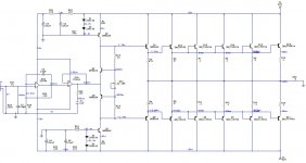
Although not quite what your going for, here is sub amp based on a USAmps design circa 1990. Rated at a measly 25 watts per channel into 4 ohms, it could be run in bridge mode into 1 ohm for 250 watts out. Since overall distortion was obviously a lesser design goal the feedback only encompassed the first opamp so there was excellent stability regardless of the mad phase shifts and inductance car subs produce since they are almost always driven around their resonance frequencies. For a full range, 8 ohm amp it could be modified by using just a single output pair and wrapping the feedback around from the output and would give quite good performance I would think. Of course the current sources could be dropped for bootstraps as well to further simplify. The bias setup works really well with the drive point in the middle making the positive and negative half very even without the need for a capacitor between the bases. Anyway just another idea for the opamp based circuits.
Attachments
It turns out that the current source was not needed. Well, it seemed like a good idea. Using a bootstrap as a kind of current source is also not needed. It benefit (according to Horowitz and Hill) is to increase the impedance seen by the VAS transistor's collector, thereby increasing its gain. And we don't have one of those.
Here is the latest version of the amp. I am still pondering that resistor between the opamp output and the negative rail. Some circuits have it and some don't. It seems to make no difference in the simulation as far as THD goes. If it puts the opamp into class A, the OPA552 can source/sink 200mA according to the datasheet. It is fully protected against overheating and even has a pin to signal when this kicks in.
According to LTspice, the circuit delivers THD of 0.0005% (yes that is three zeros) for 40W into 8 ohm at 1kHz. A pretty good number for such a basic circuit and a long way from the original in the first post. This makes me wonder just how low one can go using an opamp.
Attachments
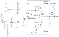
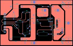
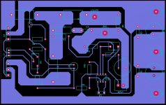
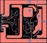
Here is the revised PCB layout. I could save a bit of copper by squeezing the components together but then again I do want construction to be easy. It is Eurocard in size (160mm x 100mm) and making it smaller will probably not achieve much.
...Except maiking everything less susceptible to oscillation, and get two boards out of the available material (I'm sure you do have some way to cut it!)
Yes, I just dug out this old thread.
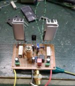
Has anybody actually built this amplifier ? Needed a cheap 30W amp and it seemed fine. Just built it on a piece of breadboard. Didn't have all the components here, so I took 0.10 R for the emitters instead of 0.15 and used MP1620 and MN2488 darlingtons instead of the TIPs. Shouldn't make any difference.
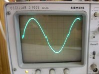
Problem is a little crossover distortion. The pic is at about 20Khz and one can see it obviously. The Vbe multiplier doesn't really work. The Trimpot doesn't do a thing. Is this thing correctly designed ? Aren't the 22K a bit to high ? Moreover I don't measure the voltages as in the spice simuation on the bases. I get about +-600mV at the darlington bases.
What can I do ? Obviously more quiescent current - but whats wrong in the schematic ?
I know how SS amp work, but I'm more into tubes and I'm lacking some experience with ss amps
Thanks
Has anybody actually built this amplifier ? Needed a cheap 30W amp and it seemed fine. Just built it on a piece of breadboard. Didn't have all the components here, so I took 0.10 R for the emitters instead of 0.15 and used MP1620 and MN2488 darlingtons instead of the TIPs. Shouldn't make any difference.
Problem is a little crossover distortion. The pic is at about 20Khz and one can see it obviously. The Vbe multiplier doesn't really work. The Trimpot doesn't do a thing. Is this thing correctly designed ? Aren't the 22K a bit to high ? Moreover I don't measure the voltages as in the spice simuation on the bases. I get about +-600mV at the darlington bases.
What can I do ? Obviously more quiescent current - but whats wrong in the schematic ?
I know how SS amp work, but I'm more into tubes and I'm lacking some experience with ss amps
Thanks
Attachments
- Status
- This old topic is closed. If you want to reopen this topic, contact a moderator using the "Report Post" button.
- Home
- Amplifiers
- Solid State
- Very simple class B amplifier