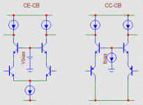
Virtually all differential input stages have a common emitter differential pair. This configuration suffers from the Miller capacitance multiplication effect, and has therefore low bandwidth.
Cascoding with a common base stage reduces the Miller effect, and increases bandwidth. This is straightforward and has been done often.
I was wondering why the common collector (emitter follower) "cascoded" by a common base stage is not used. The emitter follower inherently does not suffer from the Miller effect, but does not provide voltage gain. Therefore we use a common base stage, where the Miller effect is also absent, to provide the voltage gain. The emitter follower should be more linear than the common emitter stage...
Why has the CC-CB configuration not caught on, like the CE-CB cascode?
Has anybody any experience with it?
Attachments
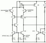
john curl said:This type of input stage was first used in the LM101 in 1966 or so.
Hello John,
I found the schematic for the LM101 on National's web site at:
http://cache.national.com/ds/LM/LM101A.pdf
I looked at it for around 3 minutes, but my head exploded before I could understand how it could possibly work. Any insights would be appreciated!
Thanks,
Charles Hansen
kyrgeo said:Why has the CC-CB configuration not caught on, like the CE-CB cascode?
Dunno. Been wondering the same about the Xfrmr/CC configuration.
se
Charles Hansen said:
I found the schematic for the LM101 on National's web site at:
http://cache.national.com/ds/LM/LM101A.pdf
I looked at it for around 3 minutes, but my head exploded before I could understand how it could possibly work. Any insights would be appreciated!
Hi Charles,
There's a PDF file at this site:
http://www.stanford.edu/class/ee214/Handouts/ho18opamp.pdf
which discusses detailed design information of the 101 among others. It's a good read.
Andy C
Warning! Off Topic Post.
Charles,
I thought you might find this a source of amusement.............
http://www.lunaticlounge.com/fringefiles/explode.html
Regards,
Jam
Charles,
I thought you might find this a source of amusement.............
http://www.lunaticlounge.com/fringefiles/explode.html
Regards,
Jam
andy_c said:There's a PDF file at this site:
http://www.stanford.edu/class/ee214/Handouts/ho18opamp.pdf
which discusses detailed design information of the 101 among others. It's a good read.
Hello Andy,
Wow! Thanks for the great link. I haven't had time to fully digest it (my head hasn't fully re-integrated after the recent explosion), but it's really, really good! Did you take this class, or did you just stumble across the file?
I still have a question. In the file you referenced, the author states, "connect the PNPs (Q3/Q4) in a differential common-base configuration".
I didn't know you could do that! Does anyone have any references for that circuit? It seems like the beta for the two transistors would have to match *exactly* for this to work. Even then, it seems a bit sketchy to me.
Thanks,
Charles Hansen
Charles Hansen said:I didn't know you could do that! Does anyone have any references for that circuit? It seems like the beta for the two transistors would have to match *exactly* for this to work. Even then, it seems a bit sketchy to me.
How 'bout if you look at the transistors as transconductance devices rather than current amplifiers as John once advised?
se
The infamous LM741 also uses this input stage. That's the only place I had seen it. The datasheet has full a schematic.
The big downside I see is the difficulty of biasing the common base transistors. You have to apply feedback to stabilise the Ibias current. Maybe this difficulty hasn't made this stage popular.
Thanks Andy, interesting link!
Mr Curl, indeed, the LM101 uses this input stage. Bob Widlar was a great pioneer in analog design!
As noone here has experimented with this topology, would there be, from a theoretical point, any advantages of this topology compared to the common differential pair?
A few simulations I have done show quite greater bandwidth and phase margin at a higher open loop gain than a comparable standard diff input, when driven by a low impedance source. This sounds good. I don't know however how the linearity compares.
The drawbacks: biasing. Due to the large gain, bias point varies wildly with tiny changes in most components. I also couldn't figure out how to apply local feedback, like the degeneration emitter resistors used in standard diff pairs.
Any ideas or comments would be appreciated!
Attachments
The circuit last posted by kyrgeo differs from the one posted first.
The latter one would be much easier to bias and implement with discretes (current source feeding collectors rather than bases !!). Degeneration resistors could easily be inserted between the emitters of each one of the two complementary cascodes IMO.
Regards
Charles
The latter one would be much easier to bias and implement with discretes (current source feeding collectors rather than bases !!). Degeneration resistors could easily be inserted between the emitters of each one of the two complementary cascodes IMO.
Regards
Charles
Charles Hansen said:(...)Did you take this class, or did you just stumble across the file?
I still have a question. In the file you referenced, the author states, "connect the PNPs (Q3/Q4) in a differential common-base configuration".
I didn't know you could do that! Does anyone have any references for that circuit? It seems like the beta for the two transistors would have to match *exactly* for this to work. Even then, it seems a bit sketchy to me.
Hi Charles,
Sorry it takes me so long to respond. I'm can only log on between 7:30 PM and 11:00 PM PST after I get home from work.
I thought you'd like that link
. I found it by accident while looking for info on the HA-5002 buffer. It seems that Google finds matches inside PDF files which is quite nice.I've only seen the differential common base thing in the old op-amps like the 101 and 741. The disadvantage as I see it is the bizarre biasing scheme for the diff amp. It's all set by the base currents of the PNPs. I disagree a bit with the "servo loop" explanation that the author uses. I think of the biasing this way:
Observe that the collector voltage of Q18 is three VBE drops above the negative supply. The supply voltage differential, together with the three VBE drops and the R1 value sets the collector current of Q18. This sets the VBE of Q18. The VBE of Q18 and the R9 value sets the collector current of Q20. So the base current of Q20 is established by the PNP beta. This base current is mirrored by Q21 and Q22 to become the sum of the base currents of Q3 and Q4. So assuming the beta of Q3 and Q4 matches the beta of Q20, the collector currents of Q3 and Q4 are each half of the collector current of Q20. So it all depends on the beta matching of Q3 and Q4 to Q20. A little flakey, but I guess it still beats the pants off of a conventional diff amp made with lateral PNPs.
I feel like I need to be re-integrated too after looking at designs like this. Reminds me of the old "Marvin the Martian" Bugs Bunny episode where Marvin gets disintegrated, then says "Being disintegrated makes me very angry!". Being nothing but a helmet and sneakers at this point, he has to waddle back into the re-integrator to get reconstituted
. Funny stuff.Folks, this is design genius in action. Bob Widlar was a design genius, and everybody in my peer group knew it. He got about 1 million $ in stock to move from Fairchild to NS. How about that? His moto was: "I'll drink to that"
If you just replace the compound input pair with a P-fet pair, you can see how it works, easier. This was essentially the UA740.
As far as the detailed writeup is concerned, this is why we go to college.
What is amazing is that the analysis is AFTER the design, by several years. In 1970, I attended a class at UC Berkeley and they did a detailed analysis of the UA741. This was a year or more, after I had used these devices in quantity in servo designs. Sort of an analysis, after the fact.
Hello Andy,
I would agree with your analysis of the biasing scheme. (It's not so bad when someone walks you through it!)
But what I've never seen before is a diff pair like Q3 and Q4. Normally the signal is input to the bases, while the emitters share a current that creates a differential action. But in this case, it seems that the signal is input to the emitters, while the bases share a current that creates a differential action.
I had never thought about this idea before, because I usually deal with FETs (and before that, tubes). I don't think this circuit would work with FETs or tubes, as there is no gate (grid) input current to create the differential action.
Now that I think about it, I guess that there is no reason why this wouldn't work for bipolars (obviously, it's been working in these op-amps for 35 years!), but it does have some distinct limitations. The bases of Q3 and Q4 are driven by a high-impedance current source, so the voltage there basically "floats" around. However, the emitters of Q3 and Q4 are "nailed down" voltage-wise by Q1 and Q2. But you couldn't replace Q1 and Q2 with a high-impedance (current ouput) differential signal source as then nothing would be nailed down for Q3 and Q4. The whole thing would be a loosy-goosy mess... (I was thinking here about ways to make a differential current-to-voltage converter that could be used for audio DACs.)
Thanks again for the link and the explanation. I think John Curl was right about Widlar -- he must have done a *lot* of drinking ("I'll drink to that!") to come up with these circuits!
Best regards,
Charles Hansen
Charles Hansen said:...I think John Curl was right about Widlar -- he must have done a *lot* of drinking ("I'll drink to that!") to come up with these circuits!
I gather Widlar was quite a character. I'll bet he had a lot of fun - laughing all the way to the bank too!
As I now see it, biasing is only difficult if you want both differential output and active loading. Single ended output with active loading (current mirror) or differential output with resistive loading are relatively easy to handle. A 10 Ohm trimpot should do the job of balancing any mismatches.
The real difficulty is to match the current of two current source loads to the current of the common-base transistors in the <1uA range. This is practically impossible...
Regarding local feedback, inserting a resistor between the two bases seems to decrease gain a bit, but it also alters the frequency response considerably, so I don't think this actually provides negative feedback.
Hi Charles, of course you can "replace Q1 and Q2 with a current output differential signal source". This is done in all normal cascoded differential pairs. The common emitter inputs have a quite high output impedance at the collectors, which are connected to the bases of the cascodes. The input impedance of the common base stage is low, so it can be considered current driven. Hope that this helps and that I have understood correctly what you meant.
I don't think it is important whether the bias for the Q3-Q4 pair is current or voltage. I used a voltage source in the simulations and it worked just as well.
Regards, Kyriakos
Hello Kyrgeo,
Actually, for cascode operation you must use a voltage source to bias Q3 and Q4. But then you lose the differential action. On the other hand, if you use a current source to bias Q3 and Q4 you will have differential action but now you lose a fixed voltage reference at the emitters of Q3 and Q4. This poses a problem for most current output audio DACs, if you were trying to make a differential current-to-voltage converter. They have a spec called "output compliance" whereby they only work properly when the output voltage is fixed within a certain range, which wouldn't happen if Q3 and Q4 were biased with a current source.
Best regards,
Charles Hansen
john curl said:Folks, this is design genius in action. Bob Widlar was a design genius, and everybody in my peer group knew it. He got about 1 million $ in stock to move from Fairchild to NS. How about that? His moto was: "I'll drink to that"
If you just replace the compound input pair with a P-fet pair, you can see how it works, easier. This was essentially the UA740.
As far as the detailed writeup is concerned, this is why we go to college.
What is amazing is that the analysis is AFTER the design, by several years. In 1970, I attended a class at UC Berkeley and they did a detailed analysis of the UA741. This was a year or more, after I had used these devices in quantity in servo designs. Sort of an analysis, after the fact.
A story related by Bob Pease was that Widlar had a fool-proof way to handle ICs that were off spec or damaged: he would Widlarise them. Widlarising involved placing the chip on a hard surface and repeatedly hitting it with a medium size hammer. THAT chip would never bother him again. Fool-proof indeed.
BTW, the Jim Williams book on Analog Design (The Art of Analog Design I think is the title) has a chapter by Bob Widlar relating how he experienced this exiting time. The whole book is great reading.
Jan Didden
- Status
- This old topic is closed. If you want to reopen this topic, contact a moderator using the "Report Post" button.
- Home
- Amplifiers
- Solid State
- A different input stage