Three amps for a 2 1/2 way speaker are much cheaper than hi grade passive crossovers
one tin foil 10µF 150 Volt (DC not AC!!) capacitor alone costs almost as much as the parts for 3 amps not to mention the even more expensive inductors. In fact BJTs resistors transfomers elcos heatsinks cost me nothing as I have those. The only expense so far is 6 complimentary pairs of On semi therm traks for 30 euros. A handful of caps opamps trimmers for 6 amps may cost another 30 euro at most and that's it for two speakers.
The most expensive of all will be the case of the speakers its a complicated design and solid hard oak.
Basically this is not new thinking anymore , the makers of active speakers are considering amp and speaker and box and acoustics of listening rooms as one system, not as independent separated devices.
If the package is considered as a system than you could easily transform it in a way to work with noninverting amp.
")
SSA can be used as inverting amp, I draw you sch in post#2392, only that in this case an input impedance drops to 1,5 kohm.
LC, also with your BIBGT HP SSA, what is the heat dissipation of input & cascode, and VAS ? If its too low then the need to more thermal compensation, and vice versa ?
Power dissipation can be calculated for each part at idle state conditions, start with input bias current level and than go gradually from part to part.
The BC5x0 have low noise and far better Vce characteristics at low voltages. The BC337/327 have even better Vce characteristics, but different gain specs. The BC5x0 should perform exceedingly well here I think.
for all BJTs of the epi planar technologies the same rule applies : the min of noise ( there are several causes of noise and several types of noise) is achieved at ic around 200 µA to 500 µA this comes combined with low fT or min of GBW and worst hfe/ic linearity. The best hfe/ic linearity and max of GBW comes at ic 10 mA. There noise has a maximum. This is just semiconductor physics. Also pnp can be made with less noise than npn.
The semiconductor designer and process engineer of BJTs has more parameters to optimize than the ones for FETs. Thus it is indeed possible to have very closely matching complimentary BJTs but not so for complimentary FETs. There are no truely complimentary junction FETs. Also complimentary
MOSFETs are impossible because of the gate source capacity. If rds on matches, the gate source capacity of the p channel must be twice as high as for the n channel. If in turn the capacities match then rds on will not match. There is no way to bypass semiconductor physics.
While power Bjts as ring emitter or multi emitter can be made perfectly complimentary if these are current driven, i.e. in terms of hfe/ic, the capacities CB , BE , are also different by around factor 2. This has to do with the majority carrier velocity , "electrons" are two times faster than "holes".
Since I was not pleased with thermal stability of this one, I tested improved CCS today. It looks that this one is going to end in SSA BIGBT HP.
Specifications are quite impressive for home DIY conditions, especially DC stability, load current regulation (1 uAmax/25°C), thermal current drift dependency (5 uAmax/25-75°C). AC performance also get a little better from previous version, noise floor is still well below -100 dB, but signal rejection ratio went down to -84 dB/100 kHz/100 ohm (8 Vpp 100 kHz sine signal according to 0,5 mVpp ripple on 100 ohm load resistor).
This one is confirmed, finally.
Attachments
Last edited:
If the package is considered as a system than you could easily transform it in a way to work with noninverting amp.
SSA can be used as inverting amp, I draw you sch in post#2392, only that in this case an input impedance drops to 1,5 kohm.
no that would not yield a CS amp.
The problem is that using the amp as inverting as you proposed , it becomes unstable as seen as ringing at square wave edges. This can be avoided by making the OL bandwidth lower
- not higher to my suprise- thus that OL bandwidth is about 20 kHz. However
as not inverting OL BW is > 100 kHz with perfect rectangle even at complex load. I think I have to have on a nice PC board to avoid any coupling or whatever effects.
only that in this case an input impedance drops to 1,5 kohm.
If non inverting i/p is grounded the inverting i/p's become one diode drop above/below virtual earths.
Feeding the i/p signal into these two offset virtual earths via the gain resistors gives an i/p Z of Rg/2 which would be of the order of about 100R
Or did I miss something ?
Last edited:
no that would not yield a CS amp.
The problem is that using the amp as inverting as you proposed , it becomes unstable as seen as ringing at square wave edges. This can be avoided by making the OL bandwidth lower
- not higher to my suprise- thus that OL bandwidth is about 20 kHz. However
as not inverting OL BW is > 100 kHz with perfect rectangle even at complex load. I think I have to have on a nice PC board to avoid any coupling or whatever effects.
If you are not really interested in the fantastic speed of this design or you have to slow it down very much to make it work well in your scheme - you seem to be moving away from the core design feature of SSA.
I think it would be much easier for you to realise your project with a different topology.
I think a folded cascode would work better if speed is of interest to you or any LTP design if it isn't.
mike
If non inverting i/p is grounded the inverting i/p's become one diode drop above/below virtual earths.
Feeding the i/p signal into these two offset virtual earths via the gain resistors gives an i/p Z of Rg/2 which would be of the order of about 100R
Or did I miss something ?
Exactly, even lower, 50 ohm (two 100 ohm parallel), me too fast, no thinking ...
If you are not really interested in the fantastic speed of this design or you have to slow it down very much to make it work well in your scheme - you seem to be moving away from the core design feature of SSA.
I think it would be much easier for you to realise your project with a different topology.
I think a folded cascode would work better if speed is of interest to you or any LTP design if it isn't.
mike
I have an even faster topology which is an inverting current feedback but with that it is difficult to take advantage of the therm trak.
curious....
Hi Hafran,
about the amp.I have been following this as they have said that it is fast...Is this mean that this amp can process a signal faster than a typical amp.If so does it guarantee or have a relation that It will provide good sonics.and can a speaker cope up with the speed of this amp.?
regards
joel
I have an even faster topology which is an inverting current feedback but with that it is difficult to take advantage of the therm trak.
Hi Hafran,
about the amp.I have been following this as they have said that it is fast...Is this mean that this amp can process a signal faster than a typical amp.If so does it guarantee or have a relation that It will provide good sonics.and can a speaker cope up with the speed of this amp.?
regards
joel
Last edited:
Hi Hafran,
about the amp.I have been following this as they have said that it is fast...Is this mean that this amp can process a signal faster than a typical amp.If so does it guarantee or have a relation that It will provide good sonics.and can a speaker cope up with the speed of this amp.?
regards
joel
the fastest electro-dynamic speakers have a rise time that equals about 20 Volts / µsec . This applies only for small excursions. And is valid for the most expensive tweeters . besides what is the max rise time that a digital sample with 96 kHz sampling frequency can reproduce? Rough estimate: One quarter of a full period takes 6 µsec. Assuming 10 Volts gives 10V/6 µsec= 1.7 Volts/µsec.
I was curious about an idea I had so I made a simulation based on the most recent reasonable schematic I could find in post 2383. I thought I would share. With some drivers for the outputs I think the GBWP could be increased. The open-loop gain is plotted without a resistive load. This was just for fun, I did not worry about thermal stability, so it needs thermal compensation before it could be built (probably facilitated by a CCS tempco).
Attachments
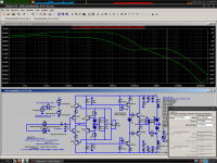
I was curious about an idea I had so I made a simulation based on the most recent reasonable schematic I could find in post 2383. I thought I would share.
Hi keantoken, thanks for sharing
3 MHz/-3db CLG is a real world repeatative result in many measurements I performed.
Did you find Q9, Q10 feedback buffers to be as improvement here, cause feedback loop is low impedance anyway. R19, R25 are also not necessary to my opinion and yes drivers makes a difference also. Not to mention VAS cascodes ...
P.S. Are Ccomp+R better performer here than usual Miller cap compensation?
Last edited:
I copied the schematic as quick as I could, I could have left out those resistors including R14 but it didn't concern me.
The feedback network may have low impedance but it got eaten up quickly with the output stage capacitances. The Cjc of the cascodes and of the outputs are the biggest limits of my schematic.
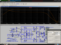
I've found that RC shunt compensation like this does a much better job at stabilizing the amp, not just this one but most amps I've simulated. This is because Shunt compensation absorbs HF energy (like a snubber), not just relocating it, potentially creating pole-mania. If you look at Miller comp and take the VAS away, you can see the miller cap injects positive feedback into the output stage. If the VAS and OPS were perfect this would not be a problem, but it is. You can exaggerate the effect if you degenerate the VAS heavily. Shunt compensation loads the input stage less at HF and is therefore also more immune to RFI. Miller compensation as it is usually applied to the VAS also decreases PSRR; Shunt compensation usually avoids this problem.
But there are some good reasons this type of compensation is not used often. #1, most people don't understand it and it's more tedious to adjust than Miller compensation. #2, it causes more distortion. With high-impedance loads it actually distorts less than Miller, but with speaker loads it distorts more. #3, Miller compensation gives the appearance of making a faster amp. In the simulator AC Analysis it looks like it but we already know Miller compensation can have trouble with RFI, and the input stage will saturate with any significant signal at those frequencies. #4, a gain hump near the -3db point is an unfortunate side-effect of shunt compensation. This is not ringing, just a hump, and it will show up as overshoot on the square wave test with it's own unique shape.
VAS shunt compensation has many practical benefits, but it's a bummer to the distortion specs. It works great but it's an "ugly duckling". Even so, I prefer it sonically over Miller compensation. It seems to have more realism, better voice legibility, and more soundstage depth. Go ahead and try it.
If you want to see a hidden example of shunt compensation, look at Symasym.
Attached is the simulated response of my circuit. Again without load. A load changes things significantly here, because the lack of buffering of the output stage. Still, it's an indicator of what can be achieved.
PS. The PSRR caveat with Miller comp could be solved by running the Miller caps to the IPS cascode emitters rather than the VAS bases. It is risky but it could perhaps be made to work.
The feedback network may have low impedance but it got eaten up quickly with the output stage capacitances. The Cjc of the cascodes and of the outputs are the biggest limits of my schematic.
I've found that RC shunt compensation like this does a much better job at stabilizing the amp, not just this one but most amps I've simulated. This is because Shunt compensation absorbs HF energy (like a snubber), not just relocating it, potentially creating pole-mania. If you look at Miller comp and take the VAS away, you can see the miller cap injects positive feedback into the output stage. If the VAS and OPS were perfect this would not be a problem, but it is. You can exaggerate the effect if you degenerate the VAS heavily. Shunt compensation loads the input stage less at HF and is therefore also more immune to RFI. Miller compensation as it is usually applied to the VAS also decreases PSRR; Shunt compensation usually avoids this problem.
But there are some good reasons this type of compensation is not used often. #1, most people don't understand it and it's more tedious to adjust than Miller compensation. #2, it causes more distortion. With high-impedance loads it actually distorts less than Miller, but with speaker loads it distorts more. #3, Miller compensation gives the appearance of making a faster amp. In the simulator AC Analysis it looks like it but we already know Miller compensation can have trouble with RFI, and the input stage will saturate with any significant signal at those frequencies. #4, a gain hump near the -3db point is an unfortunate side-effect of shunt compensation. This is not ringing, just a hump, and it will show up as overshoot on the square wave test with it's own unique shape.
VAS shunt compensation has many practical benefits, but it's a bummer to the distortion specs. It works great but it's an "ugly duckling". Even so, I prefer it sonically over Miller compensation. It seems to have more realism, better voice legibility, and more soundstage depth. Go ahead and try it.
If you want to see a hidden example of shunt compensation, look at Symasym.
Attached is the simulated response of my circuit. Again without load. A load changes things significantly here, because the lack of buffering of the output stage. Still, it's an indicator of what can be achieved.
PS. The PSRR caveat with Miller comp could be solved by running the Miller caps to the IPS cascode emitters rather than the VAS bases. It is risky but it could perhaps be made to work.
Attachments
Yes I know about this kind of serial RC compensation at input nod of the VAS. I used it already in my amps before and at a start I always put both R&C as trimmers, find the best spot in between lower and upper frequency oscillation, measure the values and solder fixed values RC parts on PCB. This kind of calibration is always fun and very acurate job, no problem to find optimum trimmers positions.
But you said that distortions are higher by this type of compensation, how much higher is that going to be?
Very nice response for both gain and phase shift, good enough for you to make it in real someday hehe
Will try it next time, thanks for the tip, regards Andrej
But you said that distortions are higher by this type of compensation, how much higher is that going to be?
Attached is the simulated response of my circuit. Again without load. A load changes things significantly here, because the lack of buffering of the output stage. Still, it's an indicator of what can be achieved.
Very nice response for both gain and phase shift, good enough for you to make it in real someday hehe
PS. The PSRR caveat with Miller comp could be solved by running the Miller caps to the IPS cascode emitters rather than the VAS bases. It is risky but it could perhaps be made to work.
Will try it next time, thanks for the tip, regards Andrej
LazyCat, any progress with GB for boards?
Hi igor0203
Well the amp is fully functional, playing music nicely, but it is still in R&D phase, so some more improvements will be tested before to go to conclusion of the project and say, this is the final SSA version.
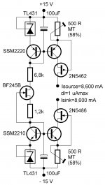
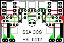
What's happening now is an upgrade for CCS current injectors to SSA feedback bridge, since it was realized that the distortion spectrum is much more clearer with the use of high performance CCSs. And these are ready to build and installed into the amps. Both positive and negative CCSs are located on PCB size 30 x 45 mm (attached) and will be soldered to main PCB as add-on module. Will look quite professionally I tell you.
Attachments
Last edited:
But you said that distortions are higher by this type of compensation, how much higher is that going to be?
At 10KHz, which I think is a frequency representing compensation quality, distortion increases from .031% to .064%. I don't know whether output drivers will bring these figures closer. Distortion at 1KHz changes only barely from .0305 to .31. This is at 12V into 6R.
Very nice response for both gain and phase shift, good enough for you to make it in real someday hehe
That sounds good to me, but right now I am invested in my own design.
Will try it next time, thanks for the tip, regards Andrej
I found 100R resistors in series with each Miller cap damped a resonance around 50MHz; could be much worse in real life.
- Status
- This old topic is closed. If you want to reopen this topic, contact a moderator using the "Report Post" button.
- Home
- Amplifiers
- Solid State
- Simple Symetrical Amplifier