Hi maxente ")
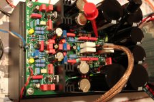
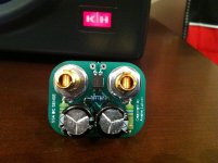
Nope, the last SSA PCB in cooperation with Alex was 198x120mm on my layout proposal and than Alex refused to go to smaller dimension. So I did it my way completely, very compact, very low Z or high speed if you like, ended at 160x120mm as you can see on pic. SSA BIGBT HP PCB layout was my design from the start.
Nope, the last SSA PCB in cooperation with Alex was 198x120mm on my layout proposal and than Alex refused to go to smaller dimension. So I did it my way completely, very compact, very low Z or high speed if you like, ended at 160x120mm as you can see on pic. SSA BIGBT HP PCB layout was my design from the start.
Thanks for answer
From the picture it looks almost the same
BTW nice design, i will build this amp some day (soon i hope ) especially whit BIGBT to test the sound
How did you came up with this configuration of bipolar and mosfet for output stage? Very interestig indeed
Sorry for those stupid questions, i am just a hobbyist


Hi guys 
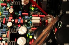
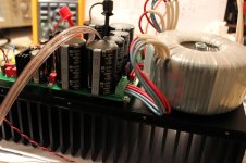
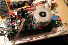
Today I finished assembly of the first SSA BIGBT HP channel, than made usual initial measurements, as everything was really just perfect, naturally I started with listening some wave music files in my lab ...
P.S. Now I am soldering another channel ...
Today I finished assembly of the first SSA BIGBT HP channel, than made usual initial measurements, as everything was really just perfect, naturally I started with listening some wave music files in my lab ...
P.S. Now I am soldering another channel ...
Attachments

......
Alex.
Hi Alex
On 27th Nov I sent you the message of mine compact PCB layout attached and you've said you won't go to so small PCB:"... because it is not all right, it is too small place to arrange all devices.", (your text - words) and than after I decided I will do it on my own.
Alex, the PCB from 30th Nov is your later version of my proposed 170x120mm layout I have sent you on 27th Nov and to which you said no. I'm sorry I really needed that dimension so I did it myself, you can see why in upper post.
P.S. On 1st Dec from your attached e-mail you still claimed it is impossible to layout in two layers, maybe in three or four ... but I did it in two layers with no vias, only pads for components.
Attachments
Last edited:
Thanks for answer
From the picture it looks almost the same
The same component layout based on my very precise hand drawn layout on mm grid paper, which BTW I always keep by myself, but completely different tracks route. I explained it all in upper post.
BTW nice design, i will build this amp some day (soon i hope ) especially whit BIGBT to test the sound
Thanks maxente, yes very dense component placement in terms of an amplifier design but it looks I cannot help myself, I did it the same almost every time I designed a PCB for my amplifiers: ProJet Power Module, Monolith, ...

How did you came up with this configuration of bipolar and mosfet for output stage? Very interestig indeed
Sorry for those stupid questions, i am just a hobbyist
BIGBT transistor came to my idea many years ago when I realize flaws of prefabricated IGBT semicondutors like GT20D101/201 and Bryston's flaw of using all bipolar design so I made discrete BIGBT. As you can see in my schematics I always drawn it in a separate box and that's because I consider BIGBT as one transistor (gain component) only. It is inherently stable, very easy to drive (high Z/low C gate input), mosfet in the middle shares/conduct only one (automatically doubles hFE) and the same base current for both outputs, resulting in identical (same waveform) collector currents of the output BJT-s. All internal currents are well defined, adjustable, balanced and at the end it acts as one non-problematic monolitic transistor, which I tested countless times. The only selection one has to make is to match NPN/PNP output pair hFE's to +/-5%, that's all.
Andrej,
So, when are you going to offer a group buy or sell your HP SSA PCB and soft start? I'm so interested and curious to try your amp. Seems promising to me.
Regards,
Fred
Since I had oportunity to taste many of current HQ amplifiers I can assure you that this one belongs to the same category. Fredlock please wait to see end-product assembled in a case. Also this thread started more as educational one, but frankly speaking I don't know where it will ends.
Hi guys
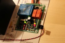
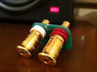
Here's my output binding posts with DC sense circuit. It triggers at +/-1,2 Vdc sending signal to SSA Soft Start C7, C8 pins, which in a case of being triggered instantly shuts down the amp's channels (high Zout), plus cuts off the power. Hopefully just won't ever happen ...
Here's my output binding posts with DC sense circuit. It triggers at +/-1,2 Vdc sending signal to SSA Soft Start C7, C8 pins, which in a case of being triggered instantly shuts down the amp's channels (high Zout), plus cuts off the power. Hopefully just won't ever happen ...
Attachments
@Salas, did you make any progress on your version? I liked your approach.
LC: any chance your build will be measured? I'm interested in distortion and noise. Before going to build anything I do want to know if it will be in "my ballpark"
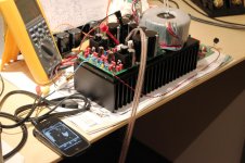
Hi Thomas
Now I'm soldering the second SSA BIGBT HP channel and this one will be measured to the last detail, so wait a little more for the specs. But as for now I can tell you there's no noise at the output at all, dead silent. I put my ear on tweeter's dome and heard no noise, hiss or whatever at all. Also no power on/off sounds, no notification from speaker, so only power LED-s on PCB or music sounds tells you the amp is on ...
LC, I'm wondering what's in that beautiful enclosure behind speaker?
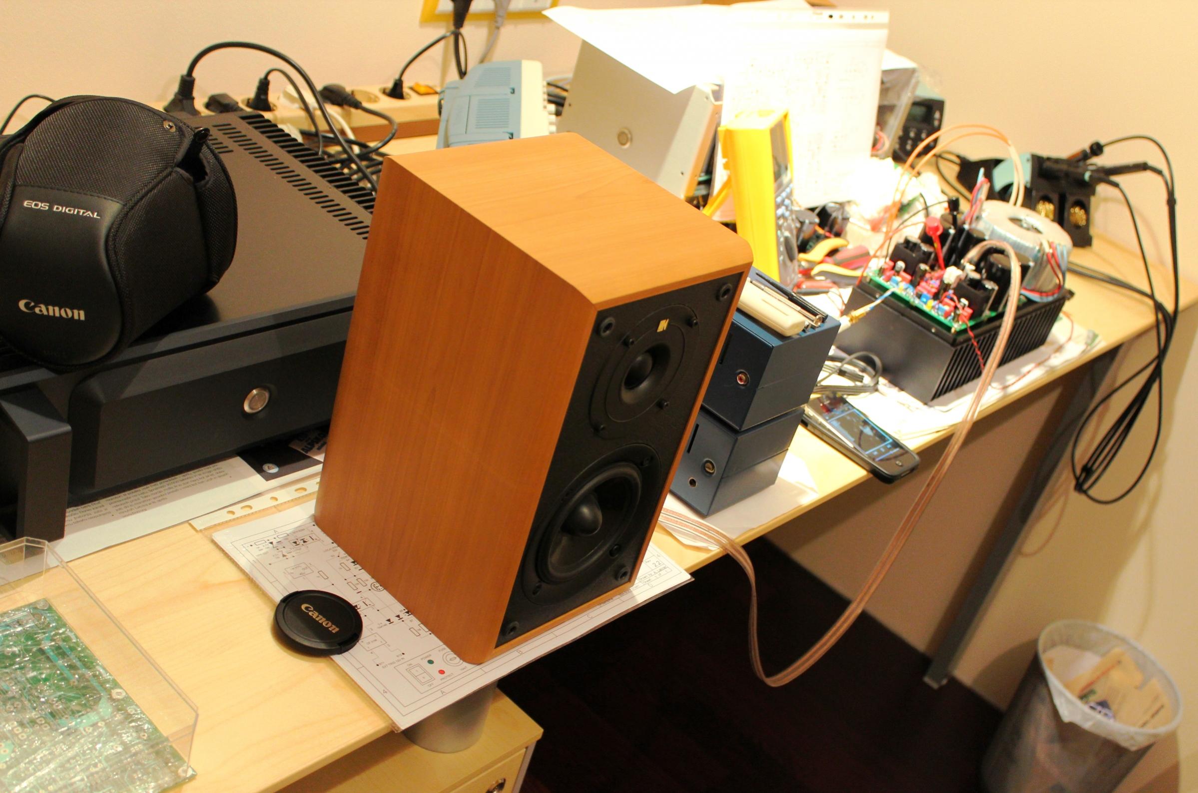
That's my StereoLith amp from 2002. In short dual mono, symmetrical LTP's VAS, 4 pairs BIGBT output, +/-80V output rails, 800VA toroid per channel. The only amp I retained for myself, all others named MonoLith (more than 20 monoblocks) were sold to my friends.
@Salas, did you make any progress on your version? I liked your approach.
Been playing very nicely but I want to see if it ''tunes up'' any further. Soon.
Hi guys
Here's my output binding posts with DC sense circuit. It triggers at +/-1,2 Vdc sending signal to SSA Soft Start C7, C8 pins, which in a case of being triggered instantly shuts down the amp's channels (high Zout), plus cuts off the power. Hopefully just won't ever happen ...
You never stop to amaze us...

Hi LC
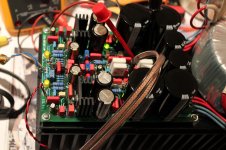
Tell me if i understand correctly i must match those two bjt transistor for close hFE from the picture below?
What about those irf's i must match them to?
Sorry if you have mentioned in other post (to mutch to read ) but how mutch power do you expect from your final version that you are building now at what load?
Attachments
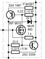
Exactly, 2SA/SC transistors should be hFE (current gain) matched inside +/-5% or even within tighter tolerance if possible but +/-5% is mandatory for good performance ie. fifty-fifty load current split between them.
Regarding IRF's matching procedure I usually perform two brief very simple measurements. First, set variable DC power supply connected to the Gate and Source of a N-channel mosfet (watch the polarity, gate is positive and source is negative) to potential that Ugs voltage causes 100 ohm Rds resistance between Source and Drain (measured with digital ohm-meter). Keep this DC Ugs voltage value to test P-channel mosfet (reverse the polarity to Gate and Source) and find the ones closest to 100 ohm Rds. Second, repeat the procedure at 10 ohm Rds among initial mosfet's selection for both channels with the same procedure like described before. What's left on the table are closely matched mosfet N-P channel pairs.
P.S. Be very careful, your body static electricity potential could easily break gate junction, +/-20V is usual Ugs max potential allowed.
Last edited:
Sorry if you have mentioned in other post (to mutch to read ) but how mutch power do you expect from your final version that you are building now at what load?
SSA BIGBT HP with +/-60V on the output stage will give something around 150W/8ohm and 250W/4ohm.
Yes they're vertical. You could try to use 2SJ79 and 2SK216 pair but these two have lower Ugs threshold voltage, different layout, plus they have negative tempco and integrated input protection zeners, but anyway it is good exchange with the same matching procedure.
Attachments
Last edited:
- Status
- This old topic is closed. If you want to reopen this topic, contact a moderator using the "Report Post" button.
- Home
- Amplifiers
- Solid State
- Simple Symetrical Amplifier