Another modification according LC comments.
For input res i will go 10k and use the input combination from LowZ with 10u cap
Marc
Hi Marc
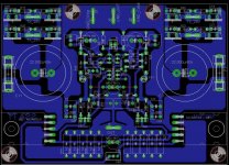
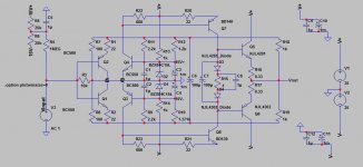
Very nice PCB layout, the placement of the C7, C22, C25, C26 is now correct, also the green LEDs are good to be on a PCB for their indicating function.
C1, C2, C3, C4, C9, C11 with their layout presence are forming some kind of EMI shield to the input from the stress field of a rectifier diodes.
You should do also GND connection split as to my suggestion on the pic, in this way C9, C11 function is max efficient (100 Hz ripple rejection).
You're now good to go.
")
Regards, Andrej

Attachments
Last edited:
You should do also GND connection split as to my suggestion on the pic, in this way C9, C11 function is max efficient (100 Hz ripple rejection).
You
I think it is good to try this kind of output stage with drivers and outputs as mosfets. Pin layout of IRF's is adequate to standard TO-220 BJT so if there will be need to change the mosfet drivers to BJTs it will be like "piece of cake" (only some minor adjustments to Vbe multiplier).
Actually I'm familiar with this output transistor arrangement, with IRF610/9610 and laterals. There is nothing wrong there, but it is not the best arrangement I believe, and the IRF610/9610 is certainly not the part I want to use there.
I have found K216/J79 only a year ago or less, so I have not enough experience with them especially in this kind of topology. From capacitance point of view the K216/J79 are fine (90pF). From other characteristics I'm not sure as these are different kind of fet than the IRF (their Vgs-on is 0.2-1.5v, much lower than even the average laterals).
In term of output "arrangement", I have judged that this topology is not the best. It is not a technical knowledge-based judgement, but it help me focus on building smaller amount of circuits.
If I have the chance to build it (the SSA_lateral with common drain output), I will compare BJT (2N5551/MPSA41) with K216, but I don't think I will be there very soon unless anyone is raving about it's better performance
You should do also GND connection split as to my suggestion on the pic, in this way C9, C11 function is max efficient (100 Hz ripple rejection).
You
LC the forum has gone out during my answer.....
I will do the modification you indicate. If work late me enough time i go for board production this month. Little more question : in the first TT schematic (that my board based on) the zener are rated 12V and in further they are rate 15V...Why?
Marc
LC the forum has gone out during my answer.....
I will do the modification you indicate. If work late me enough time i go for board production this month. Little more question : in the first TT schematic (that my board based on) the zener are rated 12V and in further they are rate 15V...Why?
Marc
- Same for feedback resistor : 1k5 instead 2k2 in first schematic.
- Should i allow more room around driver to let the possibility of mounting To220 (2sc5171/2sa1930) part for driver or To126 device will more than sufficiant for this job?
Marc
Last edited:
SSA smell
Thank You LC for Yours time and great generous will & advising all of us to follow the right Starr . . .
I implement all the suggestions You mention and I just proceed to some first beta smelling taste of SSA.
I wish You a nice Music Enjoyment times with Your nice Christmas gift . . .
Hi SOUND_Rays
I finally found the time to look over your sch and here are the comments:
- T1 should be BC560C
- input offset trimmer's +/- 15 V is provided by the existing two zeners, if the tracks on PCB will be longer than 2cm than you should also decouple +/- 15 V DC rails with 1 uF caps close at trimmers side
- I suggest you to supply front-end with +/-45 V regulated PSU to make max efficiency from the output stage swing according to supply rails
- in this case change R10, R11 to 1,5 kohm/2 W
- driver's gate DC voltage is app. 8V, so I suggest to change R19 to 2,2 kohm and P4 to 1 kohm
- VAS loading impedance is very high, there is practically no fT limitation by the load and most probable point of local oscillation, amp is also without any freq compensation, so I suggest you to put in small local feedback compensating capacitor (10-22 pF, will be practically tested) between collector and base of T9, T10 -
I think it is good to try this kind of output stage with drivers and outputs as mosfets. Pin layout of IRF's is adequate to standard TO-220 BJT so if there will be need to change the mosfet drivers to BJTs it will be like "piece of cake" (only some minor adjustments to Vbe multiplier).
Regards, Andrej
I think now you're good to go.
Thank You LC for Yours time and great generous will & advising all of us to follow the right Starr . . .
I implement all the suggestions You mention and I just proceed to some first beta smelling taste of SSA.
I wish You a nice Music Enjoyment times with Your nice
Christmas gift . . . Attachments
Thank You LC for Yours time and great generous will & advising all of us to follow the right Starr . . .
I implement all the suggestions You mention and I just proceed to some first beta smelling taste of SSA.
I wish You a nice Music Enjoyment times with Your nice
... yes R6 connect to + and add Cx to T10 also.
Thanks for all great wishes, all the best to you too.
... yes R6 connect to + and add Cx to T10 also.
Thanks for all great wishes, all the best to you too.
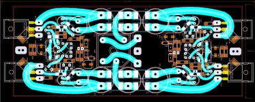
This one is in the middle of drawing phase and is a bottom layer only the top isn't displayed . . . yet . .
Need some more clear-sight nights
 to finish to the beta phase.
Really nice thank You guys for Yours sharp eyes and such great carry out with such a great precision, . . yes, sometimes long unsleepy nights easily introduce some unwanted errors... but for now all is under control . . .
My kind regards to all of You,
Tried some new value
Andrej,
because some value are hard to get here, so I prefer to re-use spare resistors I have now if possible.
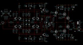
I have change resistor value in the attached schematic and seems better is frequency response in LTspice simulation. (gain linearity, group delay, phase shift)
So can you help me check the schematic and values ? hope they are good, so that I can built them. Thanks in advance
Andrej,
because some value are hard to get here, so I prefer to re-use spare resistors I have now if possible.
I have change resistor value in the attached schematic and seems better is frequency response in LTspice simulation. (gain linearity, group delay, phase shift)
So can you help me check the schematic and values ? hope they are good, so that I can built them. Thanks in advance
Attachments
Hi igor0203 
Thanks for the interest, yes, PCB-s will be ready by the end of this week, toroids, main heatsinks, Panasonic elcos, semiconductors, etc. already orderd. I'll post the pics of all the material which will be installed in SSA BIGBT HP and assembly itself, step by step. Hardly wait to get the components ...
Thanks for the interest, yes, PCB-s will be ready by the end of this week, toroids, main heatsinks, Panasonic elcos, semiconductors, etc. already orderd. I'll post the pics of all the material which will be installed in SSA BIGBT HP and assembly itself, step by step. Hardly wait to get the components ...
Hi igor0203
Thanks for the interest, yes, PCB-s will be ready by the end of this week, toroids, main heatsinks, Panasonic elcos, semiconductors, etc. already orderd. I'll post the pics of all the material which will be installed in SSA BIGBT HP and assembly itself, step by step. Hardly wait to get the components ...
Hardly waiting to see pics of your build and hear your impressions... If I'm not mistaken, you have/had access to some of best amplifiers on market and it will be interesting how your SSA will compare to them.
Yes it started, still awaiting for some parts ... The darn thing was tested and measured in so many ways-times on protoboards that there shouldn't be big problems. The layout and connections was also re-checked countless times, sooooo will see 
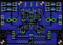
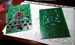
The PCB material is 2 mm thick FR-4, copper connections thickness is exactly 0,115 mm (measured), dual layer layout with metalized holes - standard quality. Maybe only the colour will be changed into deep blue later on
The PCB material is 2 mm thick FR-4, copper connections thickness is exactly 0,115 mm (measured), dual layer layout with metalized holes - standard quality. Maybe only the colour will be changed into deep blue later on
Last edited:
- Status
- This old topic is closed. If you want to reopen this topic, contact a moderator using the "Report Post" button.
- Home
- Amplifiers
- Solid State
- Simple Symetrical Amplifier