May-be this can reduce a little distortion. (see around output)
Hi Christophe, you mean reducing the trace size the feeding feedback resistor from Output point?
Marc
Edit : May be something like this attached
Attachments
Last edited:
it looks very nice
but are you sure its good to place your most sensitive curcuit right the middle of your high power supply
well, basicly its just the two rectifier bridge that bothers me
but maybe its ok
I cant see the input connection ?
but strangely, lately I see more and more members place the output devices in a way that doesnt seem to make very good use of the heatsink
and even the most experienced ones
things like having outputs at the very top of a heatsink
and I really hate when you cant turn a board 180degr, without ending up with long wires etc
sometimes its like only designing a board fore the left channel, and forgetting how both channels look when mounted
stuff like power supply connection, signal wires etc
seems like a matter of not having patience and time to think it all through, very carefully
why such hurry ?
btw, I do like that your board looks different than usual")
its 'refreshing', and good thinking
but are you sure its good to place your most sensitive curcuit right the middle of your high power supply
well, basicly its just the two rectifier bridge that bothers me
but maybe its ok
I cant see the input connection ?
but strangely, lately I see more and more members place the output devices in a way that doesnt seem to make very good use of the heatsink
and even the most experienced ones
things like having outputs at the very top of a heatsink
and I really hate when you cant turn a board 180degr, without ending up with long wires etc
sometimes its like only designing a board fore the left channel, and forgetting how both channels look when mounted
stuff like power supply connection, signal wires etc
seems like a matter of not having patience and time to think it all through, very carefully
why such hurry ?
btw, I do like that your board looks different than usual
its 'refreshing', and good thinking
Sonnya excuse me for my sad electronic knowledge, could you explain more what you mean?
Marc
You should not excuse!!! We All have to start somewhere...
In my experience, the VAS stage in this AMP changes a lot in the warmup process. So you need a constant voltage source instead so that you Can get a stable idle current
it looks very nice
but are you sure its good to place your most sensitive curcuit right the middle of your high power supply
well, basicly its just the two rectifier bridge that bothers me
but maybe its ok
I cant see the input connection ?
but strangely, lately I see more and more members place the output devices in a way that doesnt seem to make very good use of the heatsink
and even the most experienced ones
things like having outputs at the very top of a heatsink
and I really hate when you cant turn a board 180degr, without ending up with long wires etc
sometimes its like only designing a board fore the left channel, and forgetting how both channels look when mounted
stuff like power supply connection, signal wires etc
seems like a matter of not having patience and time to think it all through, very carefully
why such hurry ?
Hi,
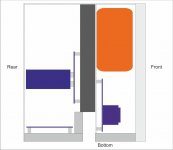
The PCB board will be place in the same orientation as in picture below (Input is in orange underlined). In the way of implamentation the output devices will be place in the first 1/3 from the heatsink bottom. The Heatsink fines will be verticaly oriented.
Attachments
btw, with cooler classAB, it would work nice mounting supply board vertically at one end of your heatsink
and please, look at size of available amp box design, height of heatsink, etc
btw, I do like that your board looks different than usual
its 'refreshing', and good thinking
and please, look at size of available amp box design, height of heatsink, etc
btw, I do like that your board looks different than usual
its 'refreshing', and good thinking
Hi,
In the way of implamentation the output devices will be place in the first 1/3 from the heatsink bottom.
them are prefect
but why not place bridge and caps 'below' them, opposite input ?
that way you would have supply line nicely placed close to bottom, and not flapping up in the upper half of your box
Tintinus,
I attached 3 internal sketch from what i have in mind : the first is a rear view, the second a front view with trafo in orange, the third a side view.
All what i built are DIY case. Dimension and configuration are always dicted by internal configuration. PSU section is in the upper parts of the board because Trafo is in taht same area on other heatsink side separated by a 2mm thick steel sheet.
Attachments
Last edited:
No, the larger, the better. I mean keeping voltage (or current) to the feedback resistor coming right from the output pin and only from there.Hi Christophe, you mean reducing the trace size the feeding feedback resistor from Output point?
Tracks are not 0 ohms and at those currents, you can see differences in signals from different points.
Tintinus,
I attached 3 internal sketch from what i have in mind
All what i built are DIY case.
ah, that is different, and clever
it is really very effective to have the heatsink go through bottom and top
I have experienced problems when having trafo close to input
but I guess your heatsink shields it nicely
Attachments

ah, that is different, and clever
it is really very effective to have the heatsink go through bottom and top
I have experienced problems when having trafo close to input
but I guess your heatsink shields it nicely
The schielding is not provided by the heatsink but by a 2mm thick steel sheet that is placed between trafo an heatsink and that is connected to ground. This steel sheet goes from bottom to case top.
Marc
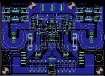
LC will you share your routing job ...
Marc
Just a little for a taste ... with Alex's permission hehe

Attachments
Duo Masters of purest Audio science of Art
Wow, what a beauty of pure Audio Art
Congratulations to both of You
Mr. Andrej for this genie beauty - Diamond,
and
Mr. Alex for Yours beautifully mastered painting of it.
The pure duo virtuoso masters of art.
-----------------------------------------------------------------------------------------------------------------
LC, Have You maybe just take a look to post #1492 and quick look to a SCH Image and possibly confirm it?
Thank You,
Just a little for a taste ... with Alex's permission hehe
Wow, what a beauty of pure Audio Art
Congratulations to both of You
Mr. Andrej for this genie beauty - Diamond, and
Mr. Alex for Yours beautifully mastered painting of it. The pure duo virtuoso masters of art. -----------------------------------------------------------------------------------------------------------------
LC, Have You maybe just take a look to post #1492 and quick look to a SCH Image and possibly confirm it?
Thank You,
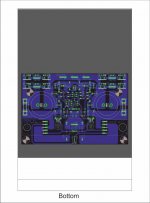
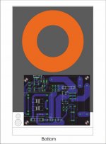
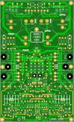
Good news : the NJL4302DG i was wating for are under way. My ThermalTrack version will use couple of NJL4281DG/NJL4302DG. I put you under the latest pcb version board. Don't hesitate to comment It.
I like very much. Just a couple things. Would it be possible to replace the output resistors (5 pairs) with a short length of straight nichrome wire? And how do you envisage connecting the output transistors to the heat sink? Would it be better to mount them off the board (hanging over the edge?).
What about splitting the power supply, so that just the output transistors are fed by a separate high power version, and the rest of the circuit fed off the on board?
I want to build them as two monoblocs, any problems you see with that?
regards
Bryan
Last edited:
Hi bryan,
I don't understand all what you say. What do you mean by "short length of straight nichrome wire"?
This project as for to goal to test SSA topology for sound evaluation in a simple compact form. This pcb board was developped according to my specifics requierements (as to use my 330va2x25V trafo, my screw 22.000µf/40v smoothing caps, Mur1560 rectier diode, 195x150x27mm heatsink...). As i said above the form must be as compact as possible (250x250x200mm at this time). Due the simplicity i expect i don't want to split Output power stage and imput power stage. This will the subject in a SSA High perf. version (BIGBT normally). In my pcb board Output device are mounted under board. If you take a look to previous case sketch you can have an idea of my project.
Marc
Hi Marc
nichrome wire is made of Nickel and Chromium, and has a relatively high resistivity, and therefore resistance, depending on diameter.
Look here for typical values: wires.co.uk : Bare Nickel Chrome / Nichrome Section
I think I am correct in thinking the output resistors should be non inductive? so typical wire wound resistors are not appropriate, but straight short pieces of nichrome would be perfect.
Will you be making the pcb's available for others?
The fact of replacing the one 0r22 5W by five 1r2 1w is due to the fact that i have difficulties to find localy 0r22 5W non inductive resistor, so if your Nichrome wire is non inductive and you can achive 0R22 (you will need to mesure the resistance value with an another methode than DMM since they completely out of value with small value) that go for. If some is interested i will share, only for DIY destination, my work since it is based on others work (LC and alex_mm) and its for me only a hobby. But all that work need to be tested for eventually debuging.
Marc
Marc
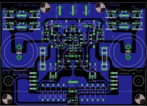
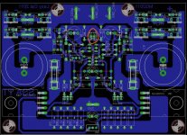
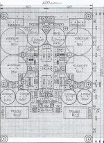
SSA BIGBT HP PCB LAYOUT Optimization
Hi tinitus
No hurry here, the more time we spend, the more quality we get, usually. So I prepared completely new PCB layout proposal according to some remarks, which brings:
- smaller PCB dimensions of only 120 mm x 170 mm
- shorter tracks, more HF ready, very-high speed design
- output transistors in the middle, better heat spread to the centre of the heatsink
- before free area above output transistors is now used for the parts,
- optimization of the board space makes more dense population, more compact PCB
- grid is 1 mm x 1 mm and shows 0,5 mm accuracy of parts placing on the layout
- there are 7 fixation M3 holes
- there are 10 through PCB holes of 6,5 mm diameter
- double layer 2 mm thick PCB
In the pic you can see the "working design" in a phase before Alex gets it to his "hands". Can be educational to some DIY newbies.
Regards, Andrej
... but strangely, lately I see more and more members place the output devices in a way that doesnt seem to make very good use of the heatsink
and even the most experienced ones
things like having outputs at the very top of a heatsink
and I really hate when you cant turn a board 180degr, without ending up with long wires etc
sometimes its like only designing a board fore the left channel, and forgetting how both channels look when mounted
stuff like power supply connection, signal wires etc
seems like a matter of not having patience and time to think it all through, very carefully
why such hurry ?
Hi tinitus
No hurry here, the more time we spend, the more quality we get, usually. So I prepared completely new PCB layout proposal according to some remarks, which brings:
- smaller PCB dimensions of only 120 mm x 170 mm
- shorter tracks, more HF ready, very-high speed design
- output transistors in the middle, better heat spread to the centre of the heatsink
- before free area above output transistors is now used for the parts,
- optimization of the board space makes more dense population, more compact PCB
- grid is 1 mm x 1 mm and shows 0,5 mm accuracy of parts placing on the layout
- there are 7 fixation M3 holes
- there are 10 through PCB holes of 6,5 mm diameter
- double layer 2 mm thick PCB
In the pic you can see the "working design" in a phase before Alex gets it to his "hands". Can be educational to some DIY newbies.
Regards, Andrej
Attachments
Member
Joined 2009
Paid Member
In the pic you can see the "working design"
Regards, Andrej

120mm fits perfekt in a modu 4U/300 with 165mm internal height, giving a nice chunky look
and those heatsink should make it indestructable in any load
- Status
- This old topic is closed. If you want to reopen this topic, contact a moderator using the "Report Post" button.
- Home
- Amplifiers
- Solid State
- Simple Symetrical Amplifier