Lasy Cat, sorry for your mistaken name....and thanks for answer. 50V. 0.5A per rail are the just power rating Or it could be less? I haven't tranny with so such output but i have 2 nice Rcore 500va 2x36V...
Marc
50V/0,5A is the VAS power supply, so it will suck few Watts only and can be also only 50V/0,1A, but the secondary winding wire diameter must withstand 4.700 uF capacitor charging current at power-on phase.

Lazy Cat.
It`s a clever little circuit you have made there!
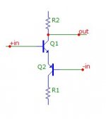
To alter the gain, the only resistors to change is feedback resistors, or do I have to change the ground resistors as well.
Global closed loop voltage gain is related to ratio 2k/100+1, so in your case 21. Open loop voltage gain is another story involving Re, Rc, VAS source impedance, etc.
P.S. Leave 100 ohm GND resistor as it is. If you change the values of the four current feedback resistors you change the fb loop current and therefore you influence the frequency bandwidth too. Please see the CF amplifier references in Wikipedia.
Last edited:
Is it +1?
What if the resistors in the NFB were 1k & 2k. Is the gain 2times or 3times?
It is +1
In a case of 1k and 100 ohm feedback resistors the output voltage is exactly eleven times higher than the input voltage, please find it for yourself, it is logical.
Your example: 2k/1k+1=3 (times)
Last edited:
Andrew,
cast you mind to the late 70's early 80's, I cannot remeber the guy's name but he introduced the differential amp made of P and N transistors. Maybe Hugh can recall his name.
Regards
Nico
I was waiting for a chance for ask if SSA input stage suitable for modifying it to a differential input stage without referencing the signal to ground. Maybe this will benefit avoiding a cap at input for blocking possible dc.
Last edited:
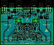
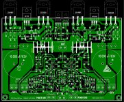
...... PCB without relay , maybe more elegant , and with larger heatsink
I expect QC to do the job , and I will post PCB rev 1.8 in B&W .
Alex.
QC started ... now
Here is a circuit that uses the Rush Cascode :
http://gaedtke.name/SubMenu_Verstaerker/KompDiffAmp-Dateien/KompDiffAmp.pdf
http://gaedtke.name/SubMenu_Verstaerker/KompDiffAmp-Dateien/KompDiffAmp.pdf
...... PCB without relay , maybe more elegant , and with larger heatsink
I expect QC to do the job , and I will post PCB rev 1.8 in B&W .
Alex.
QC report:
- face BJT's in left current source like on the right
- resistor between 4,7V and 15V zeners is 2,2k/2W (two)
- 1uF capacitor between 4,7V and GND is missing (two) – very important GND decoupling (to input GND)
- parallel to 10.000uF put also decoupler cap 1uF/63V – 5mm pin dist
- IRF gate resistors 000 are actually 47ohm degeneration resistors (silk change)
- please put 2 oposite gate protection zeners on each IRF like in SSA Basic, I will put them in sch later
- IRF9610 Source and Drain are mixed, it should be the Source to Base 2SA1987 and Drain to Base 2SC5359
- GND (SPK -) faston in between existing GND connectors is missing
- this SSA is more powerful than SSA Basic, so all the output traces should be thicker
That's the report from QC department.
Alex you are the best, regards Andrej
Nico, post 548 is a Rush Cascode.
Thanks.
...... PCB without relay , maybe more elegant , and with larger heatsink
I expect QC to do the job , and I will post PCB rev 1.8 in B&W .
Alex.
Great boards latest ones alex! Especially without the diodes and output relay (although easily jumpered). I'm liking the higher voltage. +-50V is what I've got available to use, and I want to build this version (+-50V BIGBT). But, I don't have the +-60V for the front end.
Great boards latest ones alex! Especially without the diodes and output relay (although easily jumpered). I'm liking the higher voltage. +-50V is what I've got available to use, and I want to build this version (+-50V BIGBT). But, I don't have the +-60V for the front end.
Here you have the proposal for +/-60V for SSA front-end power supply. Actually it is complete power supply for one SSA BIGBT High Performance channel.
- Status
- This old topic is closed. If you want to reopen this topic, contact a moderator using the "Report Post" button.
- Home
- Amplifiers
- Solid State
- Simple Symetrical Amplifier