I would much prefer two capacitor-banks one bank driving the output and one bank with diode separation driving the other stages...then PSU sag will only affect the output stage.. to me this clearly improves the amplifier...
I agree but please draw these diodes from the main rails and add DC smoothing caps for the input stage, than you will see that in this amp this is really not necessary, since we only have to supply DC current to one - zener potential and this can be done in the same manner like you mentioned, just with adding more capacitance in parallel to zener diodes.
")
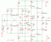
SSA complete BJT version
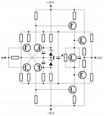
As we agreed with Nico that there should be three versions of SSA (Simple Symmetrical Amplifier), regarding output buffer, presented for listening tests:
- BJT driver/BJT output
- BJT driver/MOSFET output
- MOSFET driver/BJT output
Here is my sch proposal for the first one from the list. I intentionally left blanks for the values so we can have something to discuss about here. My only suggestion would be about the currents: input pair 2-5 mA, driver current 15-20 mA, output current 100-250 mA. Defining these currents will lead to proper resistor values, types of BJT's, etc. Any comments?
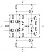
Attachments
How should the 4 input devices be thermally coupled to gain best resistance to varying output with variations in ambient temperature and operational dissipations?
Thinking about Roender's amps, he used some diodes to provide some temperature compensation for the input stage. Can we gain similar performance advantages doing something similar?
Thinking about Roender's amps, he used some diodes to provide some temperature compensation for the input stage. Can we gain similar performance advantages doing something similar?
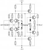
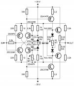
Input stage is in a perfect temperature balance regarding symmetry if the two input BJT's are in thermal contact - tested. Cascodes are non critical, drivers should be separated from the main heatsink - small, almost constant power dissipation, outputs are compensated with Vbe multiplier, so thermally looking everything is in order.
Last edited:

Member
Joined 2009
Paid Member
Offset trimmer was missing, now output DC OK.
I like it in BJT-only form, this has every chance to be a popular circuit.
I find the way you have drawn the schematic adds to the interest for me, not sure I can explain, but it looks nice
These values are of course discussable, cause now I see that the second stage (driver) voltage gain should be significantly higher, so substantial reduction of 22 ohm emitter resistance must be done. Recalculation in progress ...
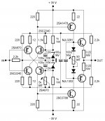
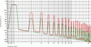
A good option would be to simply implement a double EF
as output stage , reducing THD efficently , as displayed
in the following graph.
IQ is about 0.42A in both cases.
Attachments
A good option would be to simply implement a double EF
as output stage , reducing THD efficently , as displayed
in the following graph.
IQ is about 0.42A in both cases.
I know but than we are a little out of the concept.
Please recheck THD with these new values.
Attachments
I know but than we are a little out of the concept.
Please recheck THD with these new values.
This is better but still more than 20db higher THD
than with a double EF final stage.
The VAS is really too much loaded and this ruin this circuit
capabilities wich are quite good given the schematic simplicity.
Good work , Lazycat , anyway...
It looks in this concept with 8 transistors, lateral MOSFET output's would give the best THD figures, loading the VAS less than other versions.
MOSFET driver is another option, maybe ... the best solution of this simple concept lies in the right driver/output configuration, as we have already discussed here.
MOSFET driver is another option, maybe ... the best solution of this simple concept lies in the right driver/output configuration, as we have already discussed here.
Last edited:
- Status
- This old topic is closed. If you want to reopen this topic, contact a moderator using the "Report Post" button.
- Home
- Amplifiers
- Solid State
- Simple Symetrical Amplifier