If I want to use 4 of 5 pairs of output laterals, what should be changed?
One pair of output devices is quite sufficient for the output power of this amp (40 watt). I have not seen anyone complaining of having trouble that built the Goldmund clone and discarding source resistors. I have paralleled 2SK1058/2SJ162 in the past not using source resistors and load sharing presented no problem.
Finally I am back at home and I see that very nice activity is going on here, especially someone had a lot of work, Alex you outperformed yourself, I am amazed, PCB 1.3 version is a pearl beauty. 
Me too, in all kinds of versions future will bring. What is important that I presented to DIY is splitted current feedback loop enabling proper DC working point conditions of the input BJT pair and symmetrical input diff-amp modulation with the output FB signal. In this way the input diff-amp is modulated with evenly splitted (symmetrical) distribution of the feedback signal, thus leaves no chance to the input transistors to oscillate by any kind of parasitic resonant frequency.
Implementation of this basic FB core to any kind of amp is limited just by someone's imagination.")
I Like this amp a lot. I like laterals anyway and i sometimes need a little compact amp. When it is ready i will build it. Keep the Laterals at the output. That is the charm. Even the first version. Great work on the PCB by the way. It looks really tidy.
Me too, in all kinds of versions future will bring. What is important that I presented to DIY is splitted current feedback loop enabling proper DC working point conditions of the input BJT pair and symmetrical input diff-amp modulation with the output FB signal. In this way the input diff-amp is modulated with evenly splitted (symmetrical) distribution of the feedback signal, thus leaves no chance to the input transistors to oscillate by any kind of parasitic resonant frequency.
Implementation of this basic FB core to any kind of amp is limited just by someone's imagination.
Attachments
I realy want too build this amp.
i have got plenty of 2sc2240/2sa970.
The 2sk1058/2sj162 is quite pricy at my lokal suplyer,35-40 dollares each
Is matching neaded of output pairs?
What VA rating will be a suitrable tranformer for monos?
I will try too etch my own pcb.(as soon as layout is ready)
Thanks Lazy cat,Nico and Alex for your nice work.
You can get them at Notebook, PC Zubehör, Festplatte und Elektronik bei Reichelt for around 3.5€
i hope they ship internationally with not too much shipping cost.
i hope they ship internationally with not too much shipping cost.
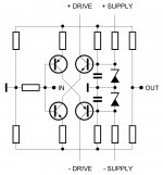
I redrew Juma's circuit schematic, one more time. The redrawn schematic (finally) made the circuit's operation obvious, to me at least.
- It's a two stage amplifier, both stages provide voltage gain
- First stage is a cascoded BJT common-emitter amplifier
- Second stage is a common-source MOSFET amplifier
- (R3, ZD1, C2) and (R4, ZD2, C3) create DC bias voltages of +15 and -15 for the cascodes
- Negative feedback is applied to the emitter of the first stage
Attachments
Member
Joined 2009
Paid Member
transistormarkj, you might find it interesting to read up on how the Nelson Pass F5 amplifier works, it's of similar topology to what you have drawn and his articles on the topic are well written. However, I'm not sure that what you've drawn matches what was posted at the start of this thread - I'll have to think about it.
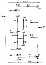
AAAAA-AND, the drawing prompts the question: What if the MOSFET output transistors Q1 and Q2 have different "threshold voltages" (VGSon) or different transconductances gm ? There doesn't appear to be a way to trim the positive (P-MOS) side, independently of the negative (N-MOS) side. Please, if I am mistaken, point out the error. Viciously and without remorse.
FYI,
I have 50 pairs of 2sk1058/2sj162 that I am about to start matching. Price will be based on yield,but could be $8-10
Interested in 4 (Four) pairs please if the cost is per pair!
--gannaji
One surprise that emerges from this drawing but not its predecessors, is: capacitor C4 is connected across two nodes that are perfectly in phase. So the AC current flowing in C4 is: zero. I didn't realize that until seeing this drawing.
Welcome to the thread, you're invited to built SSA (PCB V1.3) to share your listening experience with us.
Yes there is 1,2V DC potential across R16/C4 defining bias conditions, but when FB signal modulation starts, this potential tends to change because R11 & R12 are not current generators and there is also a hFE difference in input pair, so to keep this potential unmodulated DC the C4 is needed as a simple solution.
AAAAA-AND, the drawing prompts the question: What if the MOSFET output transistors Q1 and Q2 have different "threshold voltages" (VGSon) or different transconductances gm ? There doesn't appear to be a way to trim the positive (P-MOS) side, independently of the negative (N-MOS) side. Please, if I am mistaken, point out the error. Viciously and without remorse.
Please see the post #36 where R12 from you sch is changed with 2k trimmer to balance the circuit to zero DC offset at the output.
You can get them at Notebook, PC Zubehör, Festplatte und Elektronik bei Reichelt for around 3.5€
i hope they ship internationally with not too much shipping cost.
Thanks for the info Gerhard, I will place an order before they run out of the stock.
Very good prices for 2SK1058/2SJ162, so good it is hardly believable that these are genuine parts.
- Status
- This old topic is closed. If you want to reopen this topic, contact a moderator using the "Report Post" button.
- Home
- Amplifiers
- Solid State
- Simple Symetrical Amplifier