Dr. H,-> You're on the same way as me,
already
collecting parts for the Balanced V12 engine for my Scintillas, and as a pudding I'll add to the collection this little marvel Headphone Amp.
Where to find the Headphone amp?
Tony
Learning PCB to best serve V12-24 engine
Well, right now evaluating various PCB softw. I have plenty of time. When I'll be in a developing progress I'll post it here for sure.
I'll go the true Balanced-diferential Acuphase monoblock way, but with enormous PSU power reserve & with hardware work also.
From all my accumulated experiences till these days the power amp must have at least 7 times more power reserve + (TO3 cans)
than it'll ever need it in any the most worst case imaginable operating condition.
This way it plays music like nice, breeze, evening-warm wind on a Cheeky Pipi Island - Being there . . .
So I'm in no hurry, step by step to each single detail, fine selection of components, Silver immersed Teflon PCBs, . . .
the same overall layout look as the most powerful Acuphase Monos (my Dreams) . . .
but with at least 3 x more powerful PSU+OPs, so no termal shut offs during driving my Scintillas. . . (Bach-Organ works)..
This time by "Kings LC" gift I'll follow all my accumulated listened-tested & seeing hardware experiences,
and make the beautiest gift to myself.
My progress would be really slow and for most diyers here the least interesting, most are happy with 3 pairs of OPS per CH
and I'm sure no one needs the 2x V12 engine per CH, except maybe Some of us here, a really rare Mohikans,
having very unusual, uncommon, needs for a power amps to driving vintage ultra-Lo impedance speakers with such a pretty ease.
I was hoping we could get boards made via GB ..., if not will have to bread board it , point to point .....
Smiley 09 ....any pics yet of the beast ..... ?
Well, right now evaluating various PCB softw. I have plenty of time. When I'll be in a developing progress I'll post it here for sure.
I'll go the true Balanced-diferential Acuphase monoblock way, but with enormous PSU power reserve & with hardware work also.
From all my accumulated experiences till these days the power amp must have at least 7 times more power reserve + (TO3 cans)
than it'll ever need it in any the most worst case imaginable operating condition.
This way it plays
music like nice, breeze, evening-warm wind on a Cheeky Pipi Island - Being there . . . So I'm in no hurry, step by step to each single detail, fine selection of components, Silver immersed Teflon PCBs, . . .
the same overall layout look as the most powerful Acuphase Monos (my Dreams) . . .
but with at least 3 x more powerful PSU+OPs, so no termal shut offs during driving my Scintillas. . . (Bach-Organ works)..
This time by "Kings LC" gift I'll follow all my accumulated listened-tested & seeing hardware experiences,
and make the beautiest gift to myself.
My progress would be really slow and for most diyers here the least interesting, most are happy with 3 pairs of OPS per CH
and I'm sure no one needs the 2x V12 engine per CH, except maybe Some of us here, a really rare Mohikans,
having very unusual, uncommon, needs for a power amps to driving vintage ultra-Lo impedance speakers with such a pretty ease.
Well, right now evaluating various PCB softw. I have plenty of time. When I'll be in a developing progress I'll post it here for sure.
I'll go the true Balanced-diferential Acuphase monoblock way, but with enormous PSU power reserve & with hardware work also.
From all my accumulated experiences till these days the power amp must have at least 7 times more power reserve + (TO3 cans)
than it'll ever need it in any the most worst case imaginable operating condition.
This way it plays
So I'm in no hurry, step by step to each single detail, fine selection of components, Silver immersed Teflon PCBs, . . .
the same overall layout look as the most powerful Acuphase Monos (my Dreams) . . .
but with at least 3 x more powerful PSU+OPs, so no termal shut offs during driving my Scintillas. . . (Bach-Organ works)..
This time by "Kings LC" gift I'll follow all my accumulated listened-tested & seeing hardware experiences,
and make the beautiest gift to myself.
My progress would be really slow and for most diyers here the least interesting, most are happy with 3 pairs of OPS per CH
and I'm sure no one needs the 2x V12 engine per CH, except maybe Some of us here, a really rare Mohikans,
having very unusual, uncommon, needs for a power amps to driving vintage ultra-Lo impedance speakers with such a pretty ease.
Please keep us informed, i'm in interested in doing a 2X V12 ( balanced correct?) i was hoping you could post pics of your current beast in the other thread started by Dr H ...
Regards,
Last edited:
Andrej, does your output RC to ground shape out any steady square-wave peak you get, or is it there as a Zobel anti load inductance general?
Hi Salas
None of these, RC's are there more like a safe guard for the mosfet output stage. It simply prevents any HF unstability by linearly going down to low Z (app. 800 ohm both in parallel at 1MHz) so VAS output is brutally HF blocked by this load - safety first when headphones are in question.
")
LazyCat, you're a very kind contributor! I had in mind to build the big beast for my Apogee Scintilla speakers, but will start with the headphone amp, to learn, to listen, to gain understanding.
Thanks again!
Ryan
Hi Ryan
Very good decision, step by step to a more complex circuitry. Wish you a "good wind" to your DIY sails.
Regards, Andrej
Andrej, once again thank You for yours "generous" contribution to the DiyAudio Community and make as available such pleasure for deep music & Soul enjoyments . . . .
====---> Lazy
Cat <---====

Thank you very much Smiley, you're so positive thinking person
That gives me a looot of energy to contribute to DIY even more in the future. Thanks again, regards Andrej
One of the most brilliant Conductors - Contributors
Mr. Andrej,
It is my real pleasure seating in the last row of the DiyAudio Orchestra and
following Your Brilliant conducting to the whole orchestra nirvana.
You were fire the light ... I will follow it silently back to the exotic Island.
Thank You forever . . .
Thank you very much Smiley, you're so positive thinking person
Thanks again, regards Andrej
Mr. Andrej,
It is my real pleasure
seating in the last row of the DiyAudio Orchestra and following Your Brilliant conducting to the whole orchestra nirvana.
You were fire the light ... I will follow it silently back to the exotic
Island. Thank You forever . . .
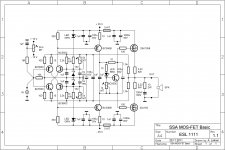
SSA MOS-FET Basic 1.1
Hi tinitus
Based on latest experiences gained from extensive tests and measurements I prepared you the SSA mosfet basic version which should work on the spot at the first time powering-up.
Instead VAS bias resistor only I put Vbe multiplier, installed on PCB, to act as adjustable zener only, to prevent DC gate voltage variations because of the VAS current thermal fluctuations. These are however small but to eliminate any bias traveling I find it most adequate, also this solution is tested and act perfectly.
VAS transistors are high voltage plus high hFE BC's because of the high bandwidth expectation from SSA. Set the VAS transistor bias current to max. 7 mA (70 mV across 10 ohm emitter resistor) to maintain its power dissipation below 250 mW.
There are also few parts added to enable input offset voltage to be trimmed to zero. Current through 1M resistor needed to balance input BJT's base currents to zero input DC voltage is only around 0,4 uA. This calibration is very important to maintain DC integrity regardless un/connected source to the DC coupled input.
Of course you can higher the rails voltages potential and recalculate two supply 1 k/1 W resistors only, but than you should be careful to speaker impedance connected because of only one pair of the mosfet outputs - SOAR.
Wish you a very pleasant time building and listening to SSA, regards Andrej
P.S. And please don't forget to thermally couple the input pair BC550C/BC560C transistors, it is very important to maintain DC offset stability.
tempting
anyone done further work on this one ?
is +/-35V highest possible voltage ?
Hi tinitus
Based on latest experiences gained from extensive tests and measurements I prepared you the SSA mosfet basic version which should work on the spot at the first time powering-up.
Instead VAS bias resistor only I put Vbe multiplier, installed on PCB, to act as adjustable zener only, to prevent DC gate voltage variations because of the VAS current thermal fluctuations. These are however small but to eliminate any bias traveling I find it most adequate, also this solution is tested and act perfectly.
VAS transistors are high voltage plus high hFE BC's because of the high bandwidth expectation from SSA. Set the VAS transistor bias current to max. 7 mA (70 mV across 10 ohm emitter resistor) to maintain its power dissipation below 250 mW.
There are also few parts added to enable input offset voltage to be trimmed to zero. Current through 1M resistor needed to balance input BJT's base currents to zero input DC voltage is only around 0,4 uA. This calibration is very important to maintain DC integrity regardless un/connected source to the DC coupled input.
Of course you can higher the rails voltages potential and recalculate two supply 1 k/1 W resistors only, but than you should be careful to speaker impedance connected because of only one pair of the mosfet outputs - SOAR.
Wish you a very pleasant time building and listening to SSA, regards Andrej
P.S. And please don't forget to thermally couple the input pair BC550C/BC560C transistors, it is very important to maintain DC offset stability.
Attachments
Last edited:
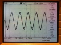
SSA BIGBT HP front-end initial power-up, stability check and some measurements.
Prior to full power testing with complete circuit (BIGBT power outputs) I checked what can I expect from SSA High Performance front-end plus power mosfet drivers. SSA input bias set to 2,5 mA, VAS bias 15 mA, drivers bias 50 mA.
Offset trimmed to zero and it was inside +/-20 mV all the measurement time with no instability issue. Bias of the drivers was completely thermally stable.
Than AC measurements took place and here are the results:
- output impedance 38 mohms, tested at 1 A/4,7 ohm load
- 1 ohm stable (drivers as output devices) inside SOAR
- bandwidth -3 dB unmeasurable with my current equipment
- input/output phase delay 12 ns at 2 MHz (period 500 ns), that is equivalent of 8,6° phase shift
I was satisfied with initial testing, so we have a go for further development.
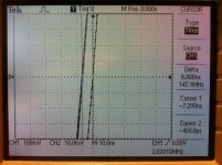
As I already explained, my current activity is mainly concentrated to the SSA BIGBT High Performance schematic from the post #1377 to squeeze out maximum performance from given topology. Here are some improvements gained from yesterday's modifications and extensive testing:
- damping factor 168 ie. output impedance 28 mohms, tested at 1 A/4,7 ohm load (IRF610/9610 as outputs in this phase of testing)
- input/output phase delay 6,8 ns at 2 MHz (period 500 ns), that is equivalent of 4,9° phase shift
- Miller-capacitance compensation capacitors of only 4,7 pF added to VAS cascodes for HF stability (small 138 MHz oscillating tendency eliminated)
In the background PCB designing process for this schematic is already in progress, so be prepared soon.
P.S. Images explanations:
- first plot shows 2 MHz output signal 22 Vpp on CH1 and 1,8 Vpp input signal on CH2, voltage gain 21,74 dB. Phase shift is so tiny that cannot be read-out from this plot
- second plot is X-Y magnified waveforms to see actual phase shift. Left rising edge curve is the input signal and 6,8 ns delayed is the rising edge from the output signal, which is BTW crystal clear from any artefacts
Attachments
Last edited:
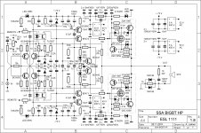
SSA BIGBT HP 1.8
Somebody would ask himself, why on this world he is performing 2 MHz testing only, what intriguing reason for that it would be?
Well, 2 MHz is only 100 times more than 20 kHz and according to my opinion, if we want to produce uncompromising power amplifier at least that 100 times higher bandwidth conditions must be well defined, only than we could expect everything is perfect inside basic 20 Hz-20 kHz bandwidth.
What I came up until now is included in the updated SSA BIGBT HP schematic.
Enjoy, Andrej
Attachments
Last edited:
Good stuff, the faster the better With my MOS amp I've worked some more on its slewrate as originally it was asymmetric. It's now a good 400V uS both pos and neg, but then again, it is driving 500W into 4Ohms and got into sub PPM region again 20 - 20KHz is/ as you describe it - pristine reproduction.
P.S. Which version of P-CAD did you draw that schematic in?
With my MOS amp I've worked some more on its slewrate as originally it was asymmetric. It's now a good 400V uS both pos and neg, but then again, it is driving 500W into 4Ohms and got into sub PPM region again 20 - 20KHz is/ as you describe it - pristine reproduction.P.S. Which version of P-CAD did you draw that schematic in?
Last edited:
+/-60V and +/-50V
LC, thank You for the fine tunning the "Master's" baby.
Please consider also the 60-50V + balanced version
for those users of PRO Installations (only) as well.
would be much appreciated.
LC it's just too bad you swap from +/-60V and +/-50V rail to +/-76V and +/-63V rail as i follow BIGBT evolution in backround...
Marc
LC, thank You for the fine tunning the "Master's" baby.
Please consider also the 60-50V + balanced version
for those users of PRO Installations (only) as well.
would be much appreciated.
Based on latest experiences gained from extensive tests and measurements I prepared you the SSA mosfet basic version which should work on the spot at the first time powering-up.
Wish you a very pleasant time building and listening to SSA, regards Andrej

hey, this is simple enough to do veroboard/hardwire
Attachments

Dear Lazy cat & others,
I've been following this thread from the beginning, since LC post the hand drawing of the SSA, since i just came in to the diy world (i'm just an accuntant) and trying to collect the knowledge from this site.
The word simplistic are catching my eye, and i like the use of bc550 since it's not hard to find in my country.
your fron end is interesting and my dumb question is "can i make a preamp by your design?
do you have the schematic for that?
Thank you
:-D
I've been following this thread from the beginning, since LC post the hand drawing of the SSA, since i just came in to the diy world (i'm just an accuntant
) and trying to collect the knowledge from this site.The word simplistic are catching my eye, and i like the use of bc550 since it's not hard to find in my country.
your fron end is interesting and my dumb question is "can i make a preamp by your design?
do you have the schematic for that?
Thank you
:-D
SSA Balanced
LC,
If implemented the needed transistors from post #846 to the last SSA Mosfet SCH, should it to be used the Fet I/P to the -3 pin XLR I/P and associated offset trimming parts also ?
Is it of any benefit to have all I/P transistors from inputs +2pin and -3pin XLR inputs to be attached together for best thermal tracking ? or is it even better to have all 8 transistors IPs incl.(cascades) on the same heat-sink to share the same tem. - follow its dependency for the complete group gain changes ?
Will this VAS stage be able to drive 2 pairs of OP LatFets ?
Thnx for the answer.
Hi tinitus
Based on latest experiences gained from extensive tests and measurements I prepared you the SSA mosfet basic version which should work on the spot at the first time powering-up.
Instead VAS bias resistor only I put Vbe multiplier, installed on PCB, to act as adjustable zener only, to prevent DC gate voltage variations because of the VAS current thermal fluctuations. These are however small but to eliminate any bias traveling I find it most adequate, also this solution is tested and act perfectly.
VAS transistors are high voltage plus high hFE BC's because of the high bandwidth expectation from SSA. Set the VAS transistor bias current to max. 7 mA (70 mV across 10 ohm emitter resistor) to maintain its power dissipation below 250 mW.
There are also few parts added to enable input offset voltage to be trimmed to zero. Current through 1M resistor needed to balance input BJT's base currents to zero input DC voltage is only around 0,4 uA. This calibration is very important to maintain DC integrity regardless un/connected source to the DC coupled input.
Of course you can higher the rails voltages potential and recalculate two supply 1 k/1 W resistors only, but than you should be careful to speaker impedance connected because of only one pair of the mosfet outputs - SOAR.
Wish you a very pleasant time building and listening to SSA, regards Andrej
P.S. And please don't forget to thermally couple the input pair BC550C/BC560C transistors, it is very important to maintain DC offset stability.
LC,
If implemented the needed transistors from post #846 to the last SSA Mosfet SCH, should it to be used the Fet I/P to the -3 pin XLR I/P and associated offset trimming parts also ?
Is it of any benefit to have all I/P transistors from inputs +2pin and -3pin XLR inputs to be attached together for best thermal tracking ? or is it even better to have all 8 transistors IPs incl.(cascades) on the same heat-sink to share the same tem. - follow its dependency for the complete group gain changes ?
Will this VAS stage be able to drive 2 pairs of OP LatFets ?
Thnx for the answer.
LC,
If implemented the needed transistors from post #846 to the last SSA Mosfet SCH, should it to be used the Fet I/P to the -3 pin XLR I/P and associated offset trimming parts also ?
The last SSA mosfet sch which is probably on your mind, I think it is the SSA Headphones Amplifier from the post #1429, if I am not wrong. Well, double j-fet buffer is sitting there just because the headphones amps shouldn't have any connectivity restrictions regarding impedance dependency issues. With input j-fet buffer SSA becomes high input impendance amplifier, suited to accept any line level audio source on the planet. If your balanced source outputs are for any reason the high impedance ones, than you should think to use j-fet buffer on both differential inputs, if not, than the regular SSA 10 k input impedance configuration is OK.
Balanced input SSA extra parts are marked with star/multiply sign, so all together 7 parts (4 trannies, 3 rebels) must be added. Trimming parts are current supply sources for complete balanced bridge, dividing current to both positive and negative input transistors, so that is where/why differentiation of the balanced signal is taking place.
Is it of any benefit to have all I/P transistors from inputs +2pin and -3pin XLR inputs to be attached together for best thermal tracking ? or is it even better to have all 8 transistors IPs incl.(cascades) on the same heat-sink to share the same tem. - follow its dependency for the complete group gain changes ?
At this point I can assure you that the best thermal stability would be if all four input transistors are on the same temperature level, 4 cascode transistors are free from this thermal joint. The best way to realize this thermal joint is to glue the flats of input transistors to each side of Al cube of 5 mm edge. Also all four of the inputs should be hFE matched within 5% of the chosen value.
Will this VAS stage be able to drive 2 pairs of OP LatFets ?
Thnx for the answer.
Yes it will be, as long as the VAS bias current is 20 mA or higher. Than of course you should take care of good heat dissipation from both VAS cascode transistors, especially because of this increased current level.
Regards, Andrej
Dear Lazy cat & others,
I've been following this thread from the beginning, since LC post the hand drawing of the SSA, since i just came in to the diy world (i'm just an accuntant
The word simplistic are catching my eye, and i like the use of bc550 since it's not hard to find in my country.
your fron end is interesting and my dumb question is "can i make a preamp by your design?
do you have the schematic for that?
Thank you
:-D
jambul, thanks for your interest for the SSA amplifier.
As sonnya already said in the post #1370 that here is no hiss at the output:
I have packed the prototype today.
...
bla bla bla
...
If the SSA was AC coupled with lower rail voltage it would make a PREAMP. There is no HISS...
you can see that you are at the right spot. Tell me some details about specs, what do you expect from your preamp: input/output impedance, gain, max. output level, etc.
The most suitable for a pream to start is the SSA Headphones Amplifier from the post #1429. What do you think?
Regards, Andrej
Last edited:
Good stuff, the faster the better
P.S. Which version of P-CAD did you draw that schematic in?
Hi MagicBox
Agree completely.
This one:
Attachments

- Status
- This old topic is closed. If you want to reopen this topic, contact a moderator using the "Report Post" button.
- Home
- Amplifiers
- Solid State
- Simple Symetrical Amplifier