Found it! Great thread. Exacly where I can ask the experts.
Please comment on the following design. Anything and everything is welcome.
I am about to build it, so creative suggestions would be appreciated.
Thanks in advance.
Hi shaan
")
I see another person who's attracted to current feedback amplifier design, good decision.
First is good to know basic topology of this kind of amplifiers and than try to make some improvements, new ideas etc.
Your kind of current mirror VAS second stage looks quite promising and conventional mosfet output buffer is also well proved. So why don't you try and make some prototype to play with the design, I'm sure something positive will come out. Beside that you will learn a lot and make step to another level to be in position to help younger less experienced builders and let the knowledge to spread on.
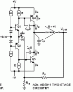
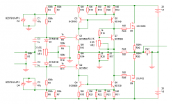
P.S. Compare your idea with attached schematic and you will see that yours is not so far away.
Attachments
Last edited:
Hi shaan
I see another person who's attracted to current feedback amplifier design, good decision.
First is good to know basic topology of this kind of amplifiers and than try to make some improvements, new ideas etc.
Your kind of current mirror VAS second stage looks quite promising and conventional mosfet output buffer is also well proved. So why don't you try and make some prototype to play with the design, I'm sure something positive will come out. Beside that you will learn a lot and make step to another level to be in position to help younger less experienced builders and let the knowledge to spread on.
P.S. Compare your idea with attached schematic and you will see that yours is not so far away.
That is the main point. As you see, I'm already on it! We'll see it working within a day or two. I am very excited with this design, I'll be happy even if it instantly oscillates and explodes! Then I'll make a second one.

Don't worry I have 500mA fuses.
THANKS for the encouragement.
Attachments
I am very excited with this design, I'll be happy even if it instantly oscillates and explodes! Then I'll make a second one.
That's the Man!


Member
Joined 2009
Paid Member
Did-you plan to use-it as guitar amp or a studio effect ?
nope - the issue is always one of moderation. I like to see that I have the option to dial in some H2 should I want it because of the desirability that has been reported for amplifiers with a 'hiraga' like monotonically decreasing profile of harmonics. Only a small amount of H2 is warranted.
Nice you have stumbled upon one of the circuits Ive used for nearly 20 years. The circuit will sound very good even without the H2 injection. The only difference is that I use feedback from the vas only, CFP vas and the output stage is openloop. Its my favourite headphone amp too although the vas is the outputstage. This circuit was first used by JLH circa 1976 and in its simplest form can be seen in the JLH MC preamp, Rega has also made use of this circuit.
I think we share some common approaches to our amplifiers. My first CFB amp was inspired by JLH designs. I'm curious about your VAS feedback because the CFB amp has a relatively low impedance feedback node which means you can load down the VAS too much of not careful - and so I see why you need a CFP VAS. I am thinking instead that I can take some nested feedback from the CFP driver stage if I want to reduce the nfb factor around the output stage and I plan to allow for this option on my pcb design.
The higher H2 from Lazycats circuit comes from the input transistors being biased at lower Vce and because of the early effect causes higher THD especially H2. Have a look at Lineup s posts of a couple of months back, there he shows the simplyfied version of this amp in a thread he started.
My own simulations show dominant H3, or at most equal H2/H3 with the all BJT version - which I don't find surprising given it's symmetry.
Parts advice
Hi All,
After reading through the thread , i decided to build this and now acquiring the parts.
As my electronic knowledge is limited, I want to build the simple version and choose easy to obtain parts.
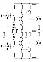
I want to build this circuit-- see attachment.
Do I choose BL or GR grade of the 2sa 970 and 2sc 2240 ?
Do I need to match the 2sk 1058 and 2sJ 162 ?
thanks
kp93300
Hi All,
After reading through the thread , i decided to build this and now acquiring the parts.
As my electronic knowledge is limited, I want to build the simple version and choose easy to obtain parts.
I want to build this circuit-- see attachment.
Do I choose BL or GR grade of the 2sa 970 and 2sc 2240 ?
Do I need to match the 2sk 1058 and 2sJ 162 ?
thanks
kp93300
Attachments
I lack the following resistors:
10ohm
33ohm
47Kohm
But have a lot of 22ohm, 100ohm and 100Kohm. After adding my laziness the prototype has become totally resistor-ed. But the values are now 11ohm, 33.4ohm and 50Kohm, which, seem to have no influence on the simulation result other than tiny gain decrease. I still lack a 33K pot, have a few 100K pots, so, maybe, ......... Noh, not a good idea; three of them will eat a lot of space-time and I can see that setting offset with them will bring hell upon me. I shall go to the shop this evening.
Picture shows the circuit I decided upon. In all my previous amplifiers the resistor-capacitor ratio was never this high. If this dude works then I'll try to make this ratio close to infinity, in the next version.
Also I plan to add a 1Kohm pot in series with the 33Kohm pot at the input. As it looks like offset voltage change is very sensitive to slider movement.
Attachments
Last edited:
It was an slightly ironic rematk about hifi. On my side, i don't like to make nice sounding equipments, i like to make transparent ones. Means to try 0 distortion, specially on the most audible side, the TIM. If we have any harmonic distortion witch gives a "nature" to the reproduced sound, better to fight against-it instead of trying to make this distortion more agreeable.nope - the issue is always one of moderation. I like to see that I have the option to dial in some H2 should I want it because of the desirability that has been reported for amplifiers with a 'hiraga' like monotonically decreasing profile of harmonics. Only a small amount of H2 is warranted.
I believe , about feedback that CF has some advantages: low impedance, that means less influence of the RF in the feedback loop, but you can do the same with tension feedback with appropriates values. So where is the secret ? In the first stage. where the feedback is applied. ANd, somewhre, because it oblige you, when you design, to think "current" witch is the only way a solid state junction think ;-)
When you use the fisrt gain stage in current feedback, with current mirrors as modulation sources, you auto compensate the all thing. Means, less the stage has gain with frequency, more it produce tension. So, if you care to build this stage with the same speed than the followings, you get a bandwidth independent from the gain factor. And, if it is faster than any signal it has to deal witn, no TIM. Only two designs are able to do this: Current feedback and errors correction, with similar results: hight bandwidth, huge slew rates.
This does not exempt us of good practices: get low distortion in open loop. Using transistors in their most linear range, reducing influence of their disparities, taking great margins in currents everywhere, and good cabling (printed boards) designs. I love the healthy and the beauty of this Lazy Cat design, because it can address very nicely those attempts, waiting with impatience his 'no compromise' solution to make that, i'm sure, will be the best amp of the moment.
How the hell is-it possible ;-)I lack the following resistors:
47Kohm.
Last edited:
Hi kp93300
Good decision to built SSA mosfet output version. You'll be awarded with very good sound coming out of your speakers.
Take BL grade 2SA 970 and 2SC 2240 and make sure that the input NPN/PNP pair will be flat-to-flat thermally coupled - very important.
At least you check Vgs at 100mA drain current from both N/P devices. They should differ not more than 25%.
Regards, Andrej
Last edited:
10k, pot 10k, 10k would gives-you less noise at this very sensitive position, and will still authorizes 30% of disparity, witch is anyway the limit ?Also I plan to add a 1Kohm pot in series with the 33Kohm pot at the input. As it looks like offset voltage change is very sensitive to slider movement.
Also I plan to add a 1Kohm pot in series with the 33Kohm pot at the input. As it looks like offset voltage change is very sensitive to slider movement.
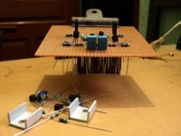
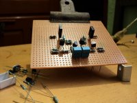
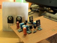
Nice proto board built, almost looks like it is ready made PCB.
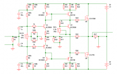
Because in your sch you provide DC bias conditions and signal drive at the input (high impedance arrangement), everything is much more sensitive to all kind of influences (thermall, potential instability/unsymmetry, ripple, RF, part's noise ...).
So for the begining I suggest you to place 15V zeners in parallel to C1, C2, replace VR1 with two 1N4148 + trimmer in series and certainly "must" is thermall coupled input NPN/PNP pair. That would help DC bias conditions to be much more stable.
10k, pot 10k, 10k would gives-you less noise at this very sensitive position, and will still authorizes 30% of disparity, witch is anyway the limit ?
You're right! Why didn't this come to me before?! Ok, As your suggested values are available in my resistor vault I will go with it. 10K, 10KPot, 10K.
Thanks for the help.
Nice proto board built, almost looks like it is ready made PCB.
Because in your sch you provide DC bias conditions and signal drive at the input (high impedance arrangement), everything is much more sensitive to all kind of influences (thermall, potential instability/unsymmetry, ripple, RF, part's noise ...).
So for the begining I suggest you to place 15V zeners in parallel to C1, C2, replace VR1 with two 1N4148 + trimmer in series and certainly "must" is thermall coupled input NPN/PNP pair. That would help DC bias conditions to be much more stable.
Wow, thanks for these points man! You may be lazy, but you are a very kind cat!
Adding the diodes, I noticed improvement in offset behaviour in the sim. Also they reduced the Iq of input and VAS, so added another 100ohm(you know where). I will thermally couple the two input BJTs. Also going to add zeners, makes sense. The voltage around the caps are 13.5V, so I thought 10V zeners would do it for me. Is 10V okay?
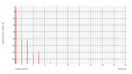
I added the distortion graph; before adding the 1N4148 diodes the third harmonic was almost 5dB higher than the second. Now they are equal in magnitude(Hope the reality be the same). What is causing it? Less Iq in input BJTs? Or better balance in Iq? I see that the current through them is +5.1mA and -5.8mA. Before adding the diodes it was +11.5mA and -13.3mA.
I have a couple more questions regarding the sim results. Here they are:
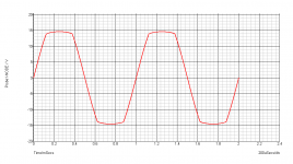
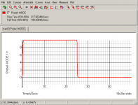
1. The clip pattern in the third picture looks like soft-clipping. Is it really so? If it is, then which part of the circuit is causing it?
2. Can you please give me hint to the slew rate from the fourth attachment? Or is it not the right graph? If not, then please tell me how to calculate it.
Sorry to ask so many questions. Thanks in advance.
Attachments
Why not feeding signal to Q1 and Q2 's inputs from the cursor of VR ? This way, you can think to suppress the serial condensers if your source has no DC ?
And, because it is not an industrial project, i would prefer to replace VR with two resistors, playing with parallels values to tune the offset. Better to have a little (little) offset than a pot.
And, because it is not an industrial project, i would prefer to replace VR with two resistors, playing with parallels values to tune the offset. Better to have a little (little) offset than a pot.
Last edited:
Why not feeding signal to Q1 and Q2 's inputs from the cursor of VR ? This way, you can think to suppress the serial condensers if your source has no DC ?
I think this way the signal will have to pass through more than 15Kohm of series resistance at the bases of the input trasnistors = lots of noise(voltage at the slider of the pot is non-zero).
And, because it is not an industrial project, i would prefer to replace VR with two resistors, playing with parallels values to tune the offset. Better to have a little (little) offset than a pot.
You already know that I have limited number of resistor values(currently). As the current through the pot is <50uA, I am okay with it. To me, it's better to have a pot than a little offset. The current schematic promises better control of the offset, this is why I want to keep it.
Last edited:
SSA Classic Current Feedback Topology
Not true. Resistance is low Zc bypassed and there is only DC measurable on the offset/bias trimmers. Look to the attached sch and play with the values. Starting points should be correct currents through different loops.
I think this way the signal will have to pass through more than 15Kohm of series resistance at the bases of the input trasnistors = lots of noise(voltage at the slider of the pot is non-zero).
Not true. Resistance is low Zc bypassed and there is only DC measurable on the offset/bias trimmers. Look to the attached sch and play with the values. Starting points should be correct currents through different loops.
Attachments
Last edited:
Not true. Resistance is low Zc bypassed and there is only DC measurable on the offset/bias trimmers. Look to the attached sch and play with the values. Starting points should be correct currents through different loops.
Thanks for correcting me. But with your suggested config there must be at least one more capacitor at either the input of the amp, or at the output of the previous stage with no volume control pot in between. How do I suppress this extra capacitor? By adding another pot may be, but I am too lazy to play and find out and also am short on space.
I re-arranged the components according to the points in your last post. I did so immediately as it made too much sense to me.
Esperado too mentioned that, IF the signal source has no DC, then I better go your way. I totally understand, But, my xover doesn't have caps at output and I don't want to add one. My preferred config is preamp to vc to cap to amp; saves headaches and I can concentrate on only the pot at the input. I already have two caps here at the input and have to get some decent film types for this app(provided it sounds acceptable initially).
I'll be grateful if you answered my previous questions.
Thanks again.
Member
Joined 2009
Paid Member
Possible an extension of this design. Here is a design I did in 2008, it has since been upgraded, And since we are exploring other avenues, here is something you guys can fine tune.
Nice design - it seems there are a lot of designs popping up in this thread - I guess there's always more than one way to skin a cat. oops, sorry lazycat,it's just an expression ...
Hi kp93300
Good decision to built SSA mosfet output version. You'll be awarded with very good sound coming out of your speakers.
Take BL grade 2SA 970 and 2SC 2240 and make sure that the input NPN/PNP pair will be flat-to-flat thermally coupled - very important.
At least you check Vgs at 100mA drain current from both N/P devices. They should differ not more than 25%.
Regards, Andrej
Hi Andrej
what size heatsink ?
200 W transformer adequate ?
Thanks for your design help and I am sure it will gives me many months of listerning pleasure.
kp93300
- Status
- This old topic is closed. If you want to reopen this topic, contact a moderator using the "Report Post" button.
- Home
- Amplifiers
- Solid State
- Simple Symetrical Amplifier