If BF471/472 transistors are replaced with faster ones from KSC/KSA series, would the amp need external compensation? The output device Gate stoppers could be redimensioned; it should enhance the bass characteristics of the amp. I have all the parts in my bin. I will first design a PCB. Thanks, Lazy Cat for such an elegant and yet simple design.
LT Spice simulation complete
I see about a gain of a bit over 19db, Idle current: P chan: 104 ma N chan:124 ma, DC out (No Signal) -167mv. This is after the bias adjust is set for around 100 ma. 8 ohm load.
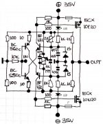
Circuit uses BC557C, BC547C inputs. MPSA42/92 "VAS" and EXC16P/N20. Yes, the big 16A output lateral fet models. No output zobel or inductor.
Clipping behavior is benign. No oscillation. Overall, a very stable amp thus far with no miller caps. Wish the gain was a bit more.
-3db at 8 MEGAHERTZ. WOW.
Phase response....the best I've ever seen but that tracks the freq. response.
I see about a gain of a bit over 19db, Idle current: P chan: 104 ma N chan:124 ma, DC out (No Signal) -167mv. This is after the bias adjust is set for around 100 ma. 8 ohm load.
Circuit uses BC557C, BC547C inputs. MPSA42/92 "VAS" and EXC16P/N20. Yes, the big 16A output lateral fet models. No output zobel or inductor.
Clipping behavior is benign. No oscillation. Overall, a very stable amp thus far with no miller caps. Wish the gain was a bit more.
-3db at 8 MEGAHERTZ. WOW.
Phase response....the best I've ever seen but that tracks the freq. response.
@Samuel Jayaraj
BF471/472 pair is just my suggestion for recommended BJT type, of course you can use faster ones like 2SA1478/2SC3788 from Sanyo or similar TO-126 low Wattage case BJT. As long as you'll be locked to proposed sch there is no need for extra frequency compensation for the cascodes cause common base is fixed to well filtered DC potential. Possible oscillation would only come from the input pair but certainly not in this current feedback configuration.
The value of the gate stopper resistors could be defined latter experimentally according to the best sounding result.
BC550C/BC560C are very good signal transistors and can be replaced to similar types but for the 2SC1845/2S992 I am not sure if noise figure is comparable, please check.
I agree design like this combined from only six transistors is nice DIY stuff.")
BF471/472 pair is just my suggestion for recommended BJT type, of course you can use faster ones like 2SA1478/2SC3788 from Sanyo or similar TO-126 low Wattage case BJT. As long as you'll be locked to proposed sch there is no need for extra frequency compensation for the cascodes cause common base is fixed to well filtered DC potential. Possible oscillation would only come from the input pair but certainly not in this current feedback configuration.
The value of the gate stopper resistors could be defined latter experimentally according to the best sounding result.
BC550C/BC560C are very good signal transistors and can be replaced to similar types but for the 2SC1845/2S992 I am not sure if noise figure is comparable, please check.
I agree design like this combined from only six transistors is nice DIY stuff.
@stoc005
Very promising LT spice results, I knew the speed of the amp would be enourmous, phase shift also the same.
Output DC offset voltage can be trimmed to zero as I already explained in post #12.
The closed feedback loop gain can be altered simply by lowering the value of 100 ohm resistors, of course both values equaly.
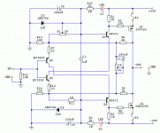
Proposed schematics has very low impedance values to the GND around the feedback loop also because of the strong feedback current symetrically spreaded to the input pair, this leave no chance to parasitic oscillations caused by the same capacitances. From there good stability of this design comes from, thus certainly deserving further investigations to be done.
Very promising LT spice results, I knew the speed of the amp would be enourmous, phase shift also the same.
Output DC offset voltage can be trimmed to zero as I already explained in post #12.
The closed feedback loop gain can be altered simply by lowering the value of 100 ohm resistors, of course both values equaly.
Proposed schematics has very low impedance values to the GND around the feedback loop also because of the strong feedback current symetrically spreaded to the input pair, this leave no chance to parasitic oscillations caused by the same capacitances. From there good stability of this design comes from, thus certainly deserving further investigations to be done.
A nice project - DIY at it's best !
Thanks Bigun
DIY if it is simple & good, makes a lot of fun. Concretely at this amp current feedback loop (really a kind of a loop) combined with bias DC potentials +/- 0,6 V is what makes it something special, very educational for the begginers.
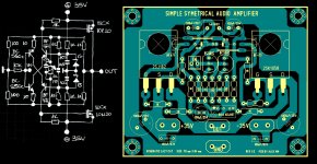
PCB for this amp could be also very simple and small especially if alex mm would take the opportunity ...
Very interesting indeed, but most of all very simple and quick to built, good job.
I was looking for a simple low power and not very expensive schematic to built an small amp and i think i have just found it, many thanks @Lazy Cat. I presume the fets can be many tipes, nut just the ones in youre desighn, as long as they present similar specifications, all should be good wright?
So despite so many amp suggestions in another thread you decided to build this one?
Member
Joined 2009
Paid Member
Only resistor devider for the bases of the cascodes in Le Monstre really can not provide any isolation from power supply ripple or DC variations, so poor PSSR is quite obvious. In my sch +/- 15 V zener filtered DC potential is substantially more adequate solution. If there would be CSS implemented instead of 1 k input pair current supply resistors, PSSR would be comparable to any CF amp.
As I already mention for such low power amps there is not a big problem to invest a little more in the power supply, which can be for this kind of current consumption even regulated to improve PSSR.
As I already mention for such low power amps there is not a big problem to invest a little more in the power supply, which can be for this kind of current consumption even regulated to improve PSSR.
Lazy Cat, thank you for your response. I think that the use of 2SC1845/2SA992 would make the amp more 'transparent' compared to BC550C/560C due to lower Cob of the former. They also exhibit higher gain. Noise should be comparable or better.
I have started with a PCB design and put the BF transistors on the ouput pair heatsink. Would it help in thermally coupling the input pair?
I take it that there is no need for a Zobel network or Output inductor, even with reactive loads. Thanks again. Wonderful design. Should soon be able to report on its sonic qualities.
I have seen SQ comparisons for BC5xx vs 2sa LTP pairs.
I don't think that the parameters (hFE & Cob) you have quoted are responsible for these SQ differences.
I have not heard the difference, but most of my amps use BC5xxc at the inputs. I have only one amp, that I am aware of, that has 992 or 1845 at the input.
I don't think that the parameters (hFE & Cob) you have quoted are responsible for these SQ differences.
I have not heard the difference, but most of my amps use BC5xxc at the inputs. I have only one amp, that I am aware of, that has 992 or 1845 at the input.
Member
Joined 2009
Paid Member
Lazy Cat, thank you for your response. I think that the use of 2SC1845/2SA992 would make the amp more 'transparent' compared to BC550C/560C due to lower Cob of the former. They also exhibit higher gain. Noise should be comparable or better.
I have started with a PCB design and put the BF transistors on the ouput pair heatsink. Would it help in thermally coupling the input pair?
I take it that there is no need for a Zobel network or Output inductor, even with reactive loads. Thanks again. Wonderful design. Should soon be able to report on its sonic qualities.
I looked over specs of 2SC1845/2SA992 and they are very promising for the purpose, only, as you probably know it, try to find as close as possible matched pair regarding hFE. Because of the simplicity of the design (not so many parts) you can easily put some extra effort to choose the best parts for the job, for instance 1% metal-film resistors, DALE, Vishay, low ESR caps Vishay, Panasonic ... When will come to the listening tests you can also try to check the BC input pair among other possibilities.
Input pair must be well thermally coupled to keep bias/offset thermall unsymetry at minimum. The best way is to glue the flat surfaces, press them firmly together to minimum the distance, wrap Al foil ribbon around them and finish with heat shrink tube to surround the pair completely.
BF pair is not so critical regarding temperature and need no extra heatsinks, power dissipation ranges from 0,09 W to 0,12 W per transistor in the worst case, so no need to mount them on the main heatsink. Also capacitance from collector to the ground is kept at minimum if we leave them alone on the PCB.
As the amp is very fast the lenghts of the connections on a PCB should be short as possible to ensure good stability through the bandwidth. But that would be no problem cause count of the material is really small.
RC serial filter to GND and possible inductor from the output can be provided at the output connectors if needed.
QUOTE=Salas;2662170]R1K under J162 better be 1K2 and paralleled with a 10K trimmer for offset control?[/QUOTE]
Yes we should put some offset control to the circuit, but the resistor changed to 2 k/Muti Turn trimmer should be according to sch attached. In this way we eqalize the currents through the input pair and balance them properly to get zero DC at output.
Also 100 ohm gate stopper resistors are there on the sch to provide some gate capacitance compensation, also to balance their values to fine tune different mosfets to VAS and to make any sound experimenting easy.
Attachments
Last edited:
An offset control should be on a final PCB IMHO. Now Alex can see the recommended way. Thanks. Are the Zeners well filtered with 100uF by the way? Takes either say 100R series resistor with each Zener to make it easier for the caps to filter more noise or bigger straight lytics to really quiet them down in my experience. Maybe he can add on final PCB too?
...... of course I have layout the first PCB
Alex.
What a smart PCB layout, very nice indeed. Thanks Alex.
As you can see some small differences took place on the sch so the board will change a little:
- gate stopper resistors added
- 2 k/MT trimmer for offset control
- two LEDs for rails power control
- fuses added
- input pair should be together with flats
- a little more space-room around BF's in a case they are vertically positioned
Please, one more 6,3 mm faston GND connection should be provided on PCB. Also the GND connection to the input should be routed directly from PWS GND faston point on the PCB to the input, where you connect 10 k together with two 100 ohm feedback resistors.
So far enough changes but Alex please stick to the approximately the same layout like it is now. Thanks again.
Last edited:
Are the Zeners well filtered with 100uF by the way? Takes either say 100R series resistor with each Zener to make it easier for the caps to filter more noise or bigger straight lytics to really quiet them down in my experience.
Feedback loop DC supply current through LED and 1k is app. 20mA. 100Hz ripple filter is formed by 1K/100uF parts who's time constant is app. 63ms if the capacitor would be ideal. There is a possibility to experiment and alter its value to max. 1000uF/16V low ESR cap to surpress the ripple to uV region on +/- 15V DC potentials, otherwise turn on phase would be just to long. So observation with scope can define the right value of these critical caps.
- Status
- This old topic is closed. If you want to reopen this topic, contact a moderator using the "Report Post" button.
- Home
- Amplifiers
- Solid State
- Simple Symetrical Amplifier