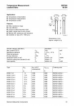
1,5 k NTC is small (3 mm disk diameter) SIEMENS negative tempco thermistor, thermally coupled to input BJT pair. Together with linearization compensation 220 ohm resistor, serves to stabilize VAS 10 mA bias current within tolerance of +/- 0,5 mA.
That's all for now, regards, Andrej
Hi Andrej, thanks for your finalized tempco config idea. We will check it out on first opportunity. Little detail please, is the disc sandwiched between the input BJTs or sits flat on their top? Thermal compound and heat shrink bundle for the 3 parts was the method? Any chance of remembering the part number of that exact NTC? Asking trivia because in compensation little things can make or break the best balance.
I probably don't understand your question...
...over-calculated to supply enough current to the gate holes capacitances of the mosfet, not ?
That is the question. The quantitative measure of "enough current", or minimum current possible. If you compare several amps I think you might agree that such topology will never give more than the average. But how can I determine the minimum value?
NB. Yes, I still have the BF stuffs, and the module is already populated with selected/matched components, also the L-shape aluminum profile, only the mosfets are in the tool box.
Hi, L.C.
I believe now, the author of the first post in a thread have now the ability to edit the first message in this forum.
May-be an opportunity to update all interesting or definitive schematics in it ?
Hi Esperado
I will do this update and some instructions to easier find some crucial points in the thread.
")
It is six months from the start and the thread grew enormously.
Regards, Andrej
SSA NTC compensation
Hi Salas
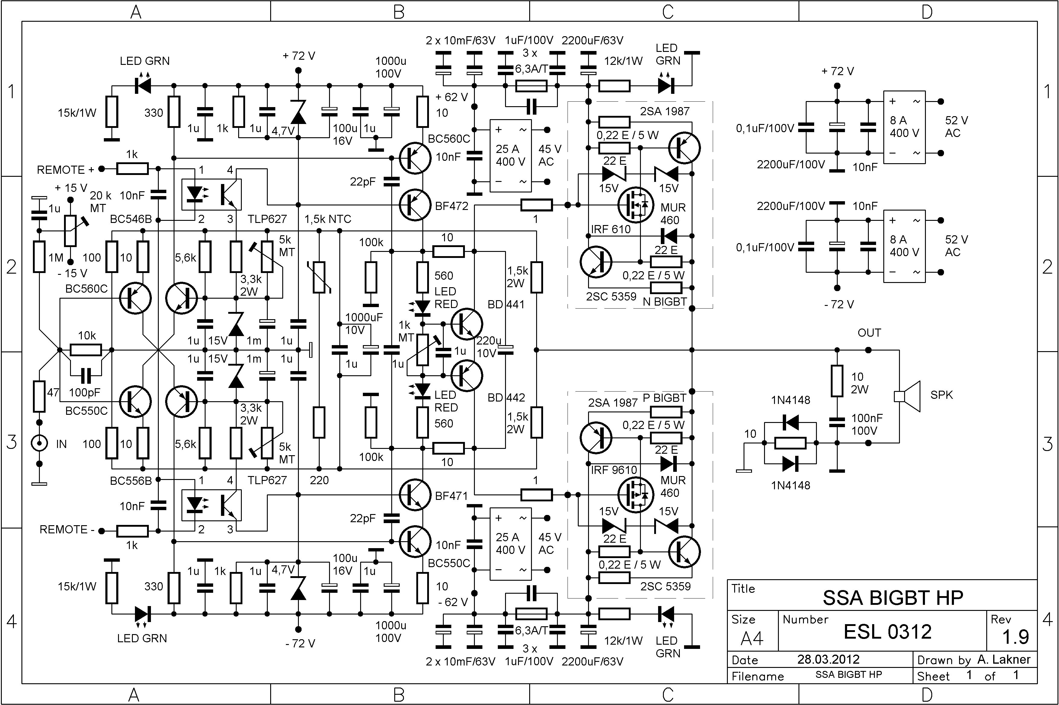
The 1,5 k NTC is from S+M (Siemens Matsushita) Components as you can see in attachment. Little instructions on this thermal compensation: input BJT pair is glued together, sides wraped around with copper foil from PCB, covered by thermal tube and on the top opening is sitting NTC. It is glued in place with one little drop of fast glue liquid, just to hold it firmly and to be in touch with BJT's plastic case. Than I covered all the BJT's top area including NTC with epoxy resin to form some sort of insulation chamber between all three parts. Compensated with 220 ohm resistor NTC follows tempco of input's Vbe precisely and thus stabilize collector current of the first stage (it is set to app. 2 mA). As a result VAS 10 mA current is also very stable although it also depends on thermal variations of the VAS BC transistor. Simple as that only two twin pin parts were added to make SSA amp reliably working. And what's best, this compensation is out of the signal path, situated in DC part of the feedback bridge.
What I'm surprised (still) is how this amp is DC offset stable. There can be +/- 20 mV DC variations on the output but that's nothing to make me act and make some sort of DC servo correction, not needed.
Remote on/off with TL optocouplers works perfectly, no unwanted sounds of any kind, only music-silence on/off. Off state is in a matter of ms after turn off, so the output stage goes to high impedance state immediately.
The schematic shows everything what's on a single double-sided PCB.
Regards, Andrej
Hi Andrej, thanks for your finalized tempco config idea. We will check it out on first opportunity. Little detail please, is the disc sandwiched between the input BJTs or sits flat on their top? Thermal compound and heat shrink bundle for the 3 parts was the method? Any chance of remembering the part number of that exact NTC? Asking trivia because in compensation little things can make or break the best balance.
Hi Salas
The 1,5 k NTC is from S+M (Siemens Matsushita) Components as you can see in attachment. Little instructions on this thermal compensation: input BJT pair is glued together, sides wraped around with copper foil from PCB, covered by thermal tube and on the top opening is sitting NTC. It is glued in place with one little drop of fast glue liquid, just to hold it firmly and to be in touch with BJT's plastic case. Than I covered all the BJT's top area including NTC with epoxy resin to form some sort of insulation chamber between all three parts. Compensated with 220 ohm resistor NTC follows tempco of input's Vbe precisely and thus stabilize collector current of the first stage (it is set to app. 2 mA). As a result VAS 10 mA current is also very stable although it also depends on thermal variations of the VAS BC transistor. Simple as that only two twin pin parts were added to make SSA amp reliably working. And what's best, this compensation is out of the signal path, situated in DC part of the feedback bridge.
What I'm surprised (still) is how this amp is DC offset stable. There can be +/- 20 mV DC variations on the output but that's nothing to make me act and make some sort of DC servo correction, not needed.
Remote on/off with TL optocouplers works perfectly, no unwanted sounds of any kind, only music-silence on/off. Off state is in a matter of ms after turn off, so the output stage goes to high impedance state immediately.
The schematic shows everything what's on a single double-sided PCB.
Regards, Andrej
Attachments
Last edited:
I have been employing a simpler idea: placing all input BJTs on one heatsink and keep the heatsink at a constant temp by means of a thermostate circuit. That requires some extra ideas on turn-on because it takes two minutes until dc offset reaches a few millivolts.
70 degrees has worked well so far.
70 degrees has worked well so far.
I have been employing a simpler idea ...
There's no simpler idea than NTC temperature compensation, since it works from cold start to hot working conditions. It compensate exact source of thermal instability in the SSA circuit - input BJT's Vbe temperature dependency.
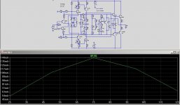
Well, as the gates are protected with resistances, you know the minimum impedance. With the hole, the resistance make a low pass filter to the signal applied to the power stage.According to the incredible bandwidth and slew rate you can simulate, made at full power, nothing to worry ;-)But how can I determine the minimum value?
Looking at the slope of the expanded square wave, you can see what i suppose is a consequence of the variation of the gate capacitance with the level, the slope goes flatter with the level (a little slower than light speed ;-).
On my side, i had tried several lower values of gate stopper, not a big difference. So i suppose we are at a nice minimum of current provided by the driver stage.
Well, one thing can be done to save some power and add some roughness would be to reduce the rail to rail voltage of the power stage ? On my size, and with my stabilized power supply, i do not wanted to complicate the wiring. May-be a switched PSU for the power stage and my PSU (with a little transformer cause less amps) for the previous one would be an ultimate solution ?
That can be reached on the average, not transients because the thermal resistance between the cases of the transistor and the junction, the high inertia of passive coolers and the low thermal inertia of the junction.In simplest words semiconductor junctions are in eternal love with constant temperature
Here too, a very fast open loop amp with enough back is the solution to minimize distortion.
Again, this remark us about reproducing music, made of transients and not about worrying about DC offsets as long as they are kept little enough.
Looking on my sims, you can see that a 10 X improvement of the bandwitch produce a factor 10 of reduction of both TIM and harmonic distortion.
That i wanted to demonstrate to myself in applying the beautiful architecture of L.C. to a promising existing amp. (That, and my lazyness ;-)
The physics behind that is "heat travels" according to laws of diffusion. These are parametrized ( i.e. solved) by constants of matter. The assumption of complete mutual independency yields exponential functions. hasn't anything to do with inertia, that is a consequence.
... Thanks for the details, now we got the whole picture. Sheldon is just ready to try that.
Yes, Thanks. Gotta order some parts. We will see if I can get the drivers to stabilize reasonably at 10mA or so. If not, I'll go with the FET outputs, so that I can run the drivers at lower current.
Sheldon
I calculated the power dissipation and from that...well using thermal conductivity - or resistance junction to case case to insulator to heatsink
yields the steady state case as all those Rth..x are solutions of differential equations for t-> infinite. The only topology that has no such problems is the Quad 303 cascade.
Thus the simulation is at best a rough estimate showing that no thermal runaway can happen.
In practice this will be tested with sine bursts at 1/2 full power where disspation is maximum and then read the current with digital scope.
http://www.diyaudio.com/forums/atta...ple-symetrical-amplifier-ssa-bigbt-hp-1.9.jpg
What is the function of the 1k resistor that parallels the 4.7V zener biasing the driver cascode? Something to do with turn on/off transients?
Sheldon
What is the function of the 1k resistor that parallels the 4.7V zener biasing the driver cascode? Something to do with turn on/off transients?
Sheldon
Hi Sheldon
Some parts of the schematic are intended to serve powering the channel, yes. Design is well tested through my many past amps and there's no easier way to turn on/off the channel without any unwanted sound transients. Yes, 1 k parallel to zener resistors serve to discharge elcos rapidly and evenly so the VAS cascodes goes to off and so are the outputs. Two 100 k resistors to GND holds the output stage to zero until it goes off completely. As you can see, because of this design solution, there is no output relay and that's what I like it.
Some parts of the schematic are intended to serve powering the channel, yes. Design is well tested through my many past amps and there's no easier way to turn on/off the channel without any unwanted sound transients. Yes, 1 k parallel to zener resistors serve to discharge elcos rapidly and evenly so the VAS cascodes goes to off and so are the outputs. Two 100 k resistors to GND holds the output stage to zero until it goes off completely. As you can see, because of this design solution, there is no output relay and that's what I like it.
- Status
- This old topic is closed. If you want to reopen this topic, contact a moderator using the "Report Post" button.
- Home
- Amplifiers
- Solid State
- Simple Symetrical Amplifier