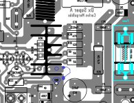
While making the pcboard to the Dx Super A i had this trouble
about the coil position.... it was too much close to the VAS transistors...and there, a huge current would cross...several amperes crossing the coil on the run to the speaker coil... a giant magnetic field would appear there.
Because of that i have asked Juan to move the second VAS heatsink in order to create a kind of wall... a kind of shield, trying to avoid the magnetic field to disturb VAS and early stages operation... one thing we did was to provide earth (ground) connection the VAS heatsink obtains a stronger shield.
Because of that problem we had three main decisions to make...or we remove the coil, or we shield the coil or we move the coil out from the pcboard.
My decision, taken into the Dx Super A board, was the shield providing ground connection to the VAS heatsink...this was the decision, because the coil remotion would never be accepted by builders and to move the coil out from the traditional, ancient and standard position would also not be acceptable.
Decisions when you make amplifiers are not only technicall decisions...they are also political decisions because your gonna try to apply methods to people...and they have their faith, their traditional beliefs about what is correct and what is wrong... we found (Juan and me) the better solution would be to shield the VAS against magnetic field from the output coil instead to move it out or to change it's position related the pcboard..... in all world amplifiers you have the coil mounted into the pcboard...so...move it out would be a scandall... and removing it a crime into folks mind.
See the image.... the heatsink has two mounting posts that goes through the pcboard fiberglass material and crossing it result in a point that can be soldered, because these pins are iron made, so, accepting solder...this way we have the heatsink fixed....the power transistor (second VAS stage) is insulated from the heatsink that goes grounded with a drop of solder or a small wire jumper soldered below the pcboard.
This shows, and proves you our concerns about the subject (see the image) and i will search for the video file to show you my instruction to Juan about the subject... if not deleted because was a series of video private messages delivered to Juan while he was preparing the layout.
regards,
Carlos
Attachments
Last edited:
You can never please everyone.
Ive tried laying out PCB, and its not easy.
Mr Juan has done a impeccable job, better than many commercial amplifiers Ive seen.
I am so thankful to all our PCB masters on this forum, that spend countless hours making PCBs for this community.
Regards
Ive tried laying out PCB, and its not easy.
Mr Juan has done a impeccable job, better than many commercial amplifiers Ive seen.
I am so thankful to all our PCB masters on this forum, that spend countless hours making PCBs for this community.
Regards
Yes Vostro...you made justice to Juan Vargas
He worked as a workhorse....have never complained...i have asked him dozen times to change things...he always did with good will, without complain.
Great guy Juan....i hope he can read your congratulations...i do think he will feel good...and he deserve that a lot.
He is a real humble man... easy going... never discuss and never try to be more clever than the circuit designer...he follow instructions and sometimes give suggestions and do not mind if we accept his ideas or not...he use to make questions to understand the reason why i ask modifications and he accept when i say "feio" that means "ugly"..he accept these non technicall things without discuss..he do think this is a good reason......nice guy...he and Mitchel were the most easy going guys..... very easy to work together Juan.... very pleasant...he never made me feel upset with him.
Here you have the nice guy face.... if i win a lottery game... 4 million dollars.... in the end of this year, i will move to USA.... and Juan will work with me into the real Dx Corporation factory.
regards,
Carlos
Attachments
Last edited:
oh man! I feel happy thank you guys this will motivate me even more to keep doing what I like the must "layouts designs" it feels good indeed guys I appreciated , that charge my batteries  thanks again! I feel like this cartoon that I like so much!
Best Regards
Juan
thanks again! I feel like this cartoon that I like so much!Best Regards
Juan
Attachments


I like my Hx so much! It's powerful, precise and punchy. It's my passtime to discover all of its subtelties and to learn on a real big fat amp how stuff works... That's why I decorticate it so much and I put it to the test so much, both sonically and on my test bench as well.
I think I've found what'S causing the dent on the downward slope that occurrs on my test bench. It seems to be caused by the VAS bootstrap. In the simulator, If I only put a CCS, the dent doesn't appear. If I put a bootstrap only, the dent is present. That dent is there while using the initial CCS/bootstrap configuration. For all the tests in simulation, I arrange to have the exact same 16mA at the VAS emittor, and to have 54mV bias.
"curious" Mart...
Mart
I agree with your philosophy? of sonic and technical assessment. I'm curious about how you simulate the dent. I have been trying to replicate it using Multisim 12 but it just won't appear. Are you using the original MK III design in your simulations with no changes other than the stopper resistors at 100r and the bias at 54 mv? Also the 16 ma VAS emitter current is lower than what I measure with a probe during simulation. Have you made any mods that would change the VAS current? I didn't see a change in VAS current when I deleted the bootstrap cap.
Not interaction with non-ferrous surroundings.
The other circuits may have a "directionallity".
If the on board coil "adds" the same directionallity then you get increased antenna/aerial effect when current values change.
If the on board coil "subtracts" from the on board circuit aerials/antennae then you may get less of feedback effect.
It is better to remove the coil from the board and instead insert it in the cable route leading to the speaker terminals.
I have been telling you this for years. Won't you listen?
Now back to the "The other circuits may have a "directionallity"."
After having located the coil OFF board, go back and design the PCB layout to minimise the feedback effects of the trace directionality.
One way to avoid this trace directionality is to ensure that all traces are paired as FLOW and RETURN.. This is the Low Loop Area philosophy.
It is this "rule" that is habitually ignored in all the DX amplifier layouts where the power inputs are on opposite sides of the PCB. The worst way to layout the Power Supplies !!!!!
Well this is good news for me since I moved the coils off board on the initial build. I guess I don't have to worry about going back in and turning them around or rewinding them. I understand how the coils magnetic field can interact with PCB traces or components and create unintended feedback. I don't understand how the direction of coil winding would make a difference here. Isn't the magnetic field polarity a function of the direction of current flow? If so how does the winding direction (presumably meaning clockwise vs counter clockwise) matter? Isn't the current flow changing direction with each transition across zero volts?
Steve
These heatsinks we buy are alloy..they are not pure aluminum
because pure aluminum is a very weak material.... too much soft, alike pure gold, reason why gold is made mixed with other material to harden up.
Really the shield used is not that effective, because non ferric material, another kind of shield should be tried to check how much this gonna be needed.
Insulated steel blades should be placed in between the coil and sensitive parts while watching the scope.... i cannot do that, my scope is damaged... to try you need a steel can and a scissor..cut it in a small rectangle, solder a wire on it and the other wire extreme goes to ground..then insulate with electrical tape and go placing into the power amplifier board while watching the scope.... finding the place..hot glued into the place and ready.
To move coils out from the board is neither simple nor practical... first because you will need extra boards to assemble coil and resistor, or they gonna be soldered floating in a ugly way into your output post...second because you will now generate intense magnetic field in other place that cannot be nearby the input connectors or the problem may become worse.
Not that clever solution i think... imagine you build a house and then a tree is covering the sunlight and the place is cold...then will you dissassemble and dismount the house to rebuilt in another place or will cut the tree?... there's an easy and a not easy solution....one is clever and other is not... i do think a try to shield is much more easy, much less ugly and produce much less work than to move the coil out from the board.... this is not a clever idea reason why i have never gave support to this exotic thing...also i imagine people will not like it too...there's an old tradition of coils inside power amplifier pcboard..to break the rule of tradition is hard, some will accept and others will not.
regards,
Carlos
Last edited:
That utilisaste for the simulation program. subier these circuits could you pobrarlao on my computer.
Greetings. SERGIO.
I do not have MKIII simulation files here at my home
Only after holidays...at january the second..
"Yo no tengo archivos de simulación ahora en mi casa ... tal vez en mi trabajo ... pero sólo puedo ver después de 02 de enero"
Email:
nanabrother@hotmail.com
carlos.eugenio1951@yahoo.com
My forum adress:
Amplificador DX • Índice
My youtube channel:
Carlos Mergulhão - YouTube
Hasta la vista... see you!
Carlos
Juan had a goog idea to fix heatsinks that does not have the fixing feature
And i made a complementary blade to increase shielding using metalic can blade.
Juan's idea complementary video - YouTube
regards,
Carlos
And i made a complementary blade to increase shielding using metalic can blade.
Juan's idea complementary video - YouTube
regards,
Carlos
The heat sink I using does not have the solder taps at the bottom last night I was thinking how to provide GND to the heat sink to protect the VAS transistor from magnetic field now mister Carlos even get a new idea of placing a piece of metal material that can be solder to the copper wire that has GND already of course this will apply more to Dx Super A but also can be done in MKIII it does not have the holes like I did to Dx Super A but it can be shielded as Carlos mention on his video, here is the video of the idea.
http://www.youtube.com/watch?v=M9Uof99W7ZM&list=UUEV_-UcnVM-o3KnQe6nemTQ&index=2 first one
Dx Super A Heat Sink ideas 2 - YouTube second one
I apologize for my horrible Spanish accent been leaving in Puerto Rico for too long lol.
Regards
Juan
http://www.youtube.com/watch?v=M9Uof99W7ZM&list=UUEV_-UcnVM-o3KnQe6nemTQ&index=2 first one
Dx Super A Heat Sink ideas 2 - YouTube second one
I apologize for my horrible Spanish accent been leaving in Puerto Rico for too long lol.
Regards
Juan
Last edited:
Mart
I agree with your philosophy? of sonic and technical assessment. I'm curious about how you simulate the dent. I have been trying to replicate it using Multisim 12 but it just won't appear. Are you using the original MK III design in your simulations with no changes other than the stopper resistors at 100r and the bias at 54 mv? Also the 16 ma VAS emitter current is lower than what I measure with a probe during simulation. Have you made any mods that would change the VAS current? I didn't see a change in VAS current when I deleted the bootstrap cap.
I've updated some components simulations parameters with the ones provided by OnSemi. I noticed that it made a difference in behavior in simulation. Anyhow, I can send you my simulation file if you wish. Just PM me your e-mail address...
Martin.
I have the new resistors now 4 x 56R and 4 x 100R.
I have also done a modification R09 390R changed to 2.2 K.
What is the value of resistance will I take for R23A and R23B, the 56R (Bonfis has installed) or the 100R (Martin has installed) ?
Regards,
Rudy
Hi Rudy-
They both work. I used the 56R because it was a small increase over the original value but still eliminated the parasitic.
Steve
Hi Rudy-
They both work. I used the 56R because it was a small increase over the original value but still eliminated the parasitic.
Steve
Hi Steve,
Have you also C10 changed from 180pf to 100pf ?
Regards,
Rudy
Attachments
Hi Steve,
Have you also C10 changed from 180pf to 100pf ?
Regards,
Rudy
Yes but I wouldn't recommend that unless you make the other change I made to the input stage. I think it would also be wise to have access to a scope to make sure the amp is stable after changing C10. I think Cannonica has C10 at 100pf also. Maybe he can comment on how his input stage is configured.
Steve
My input stage is exactly as the pic posted by BMW850. From my simulations, the increased base stop resistor let me confident to decrease the miller cap. I got no issue at all with the real thing either concerning oscillations. I only had oscillations getting out of clip without the baker clamp, but it was not relevant to Cdom value.
Mart.
Mart.
- Status
- Not open for further replies.
- Home
- Amplifiers
- Solid State
- Dx Blame MKIII-Hx - Builder's thread