Most of the time really simple amplifiers can have a huge DC offset of up to 0.1 volts or even higher depending on brand and age which is not very good at all, but with some fine tweaking, dc offset on these amplifiers can be brought down to picovolt levels. Observe that the LTP transistors should be tightly coupled together face to face, preferably with a screw based clamp, but a tight zip tie works ok, with some thermal grease to minimize offset drift due to unequal temperature.
Here is such an example:
http://i.imgur.com/8zimX.png
Of cource in reality this is gonna drift wildly over time, possibly several millivolts up and down due to air currents over components and VLF signals picked up at the input.
However minimum possible dc offset is something that should ALWAYS be strived for as it offers the best possible sound quality with minimum assymetrical distortion.
I have a commercial amplifier that has so low dc offset that it doesent even register on a digital multimeter.
That is what i use as my reference.
Here DC offset is minimized on a blameless design:
http://i.imgur.com/eqe2u.png
That is what i use as my reference.
Here DC offset is minimized on a blameless design:
http://i.imgur.com/eqe2u.png
Last edited:
Tekko,
DC offset up to about 150mV has no effect on sound quality except to displace the speaker cone slightly to one side, very slighly increasing H2 and H4. You wouldn't notice it.
Clamping LTPs together is not necessary to achieve quite adequate offset control.
Other non-linearities elsewhere in the circuit, particularly at the voltage amplifier, are far more significant than any concerns about picovolt offset control.
The big one is distortion profile.
I would not normally comment, but you seem pretty adamant about this....
Hugh
If you can achieve less than +-15mVdc of output offset (total range of 30mV) for the full range of operating conditions you will be doing well.
Neither |pV| nor |nV| from a simulation gives little clue to how all the device parameters will interact and affect output offset, as voltage and temperature changes.
Neither |pV| nor |nV| from a simulation gives little clue to how all the device parameters will interact and affect output offset, as voltage and temperature changes.
There is a fundamental problem simulating circuits like this. This is that all instances of a particular type of device are identical. This means that if the are operating at the same currents and Vce, the base - emitter voltages will be idsentical, and thus the circuit appears to has zero offsett. The solution to this is to use similar transistor but intelligently change some of the key parameters, like Bf and Is. In LTspice you can use the AKO (a kind of) feature.
Is there a "Monte Carlo" feature in LTspice?
Here you could set all the resistor to vary throughout their 1% tolerance range and see what effect that has on output offset.
Reset the resistors to "perfect" and try setting a tolerance range for hFE and run the Monte Carlo.
You could also try Vbe tolerance range.
Finally you could vary all three to see how much the offset can drift with just these three parameters changing with operational conditions.
Q.
is Monte Carlo the correct term for tolerance sensitivity simulation?
In my eyes, anything above 30 millivolts offset is wrong and possibly a sign of a badly built amplifier.
The lower the offset, the better.
I've seen this as quite acceptable on many OEM's (according to manuals).
For our DIYA LIN amps , 1-5mv (right out of the box - mouser order
") )
)- simple DMM matching.
With input pair "face to face" - as you say.. and a coupled VAS-CCS , even a 5C - 40C change in ambient temperature seems to have little effect.
2 year old amp set to .5mv might read 2-3mv worst case.
I use the crude hairdryer to make this happen real fast sometimes , even pushing 60C , a worst case 10mv.
The LIN bootstrap current source is a little worse , but not much. The cap has a less defined coefficient (still can't come close to 30mv).
AB international and ADCOM amps are harder , mostly because they are fully complimentary IPS's with 2 input pairs. These are the ones with 30mv offsets.
Very trivial , but I also like .5-1mv
(why not?)OS
Not zero in simulations
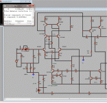
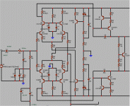
Actually , the real amp is represented quite well in the topology VS. offset category.
(below 1) shows the LIN at -5mv (exactly where most real ones end up)
(Below 2) ends up at +/- 30-50mv unless you change one of the CCS's , also just like a real one. On this type amp one would usually incorporate either a servo or direct DC bias offset at the differential(s). Of course the simulator can't account for differently sourced devices - impossible.
OS
Attachments
That is exactly what an AC coupled amplifier does. NFB tries to minimise the difference in the +IN to -IN inputs by adjusting the output. The clever bit is recognising that AC NFB and DC NFB are different and different device parameters are at work.Surely a DC offset can de dealt with in the design stage with the application of a little negative feedback, the loop being well decoupled as regards audio signals?
The symsym and similar input stages can be zeroed to within +-1mVdc and stay in that band over most operating conditions, simply because the DC operating parameters are carefully matched and the device temperatures are carefully matched by design.
- Status
- This old topic is closed. If you want to reopen this topic, contact a moderator using the "Report Post" button.
- Home
- Amplifiers
- Solid State
- Minimizing dc offset in simple amplifiers