Std. Heatsinks??
With the different PCB output device layouts, is there any guidance as to a preferred heatsink?? I tend to like the Conrad single flange style but mounting them into a suitable chassis can be "interesting".
Mounting the outputs to an aluminum "L" bracket and bolting it to a flat heatsink is not optimal either, IMHO.
A large, flat heatsink does work for some the PCBs in this thread.
Documentation
This is good.... What I need now is some suggestions on my Options/construction "manual". I just had someone that built my big "mongrel" (PB250 +AX= this amp ) , change some components to reduce total gain and produced an oscillator. I told him how to recompensate (increase input degeneration) for this or just attenuate the input signal. Someone else put semi's in backwards and let some magic smoke out
  . (all is "fixed" now )
For this kit , besides a VERY verbose BOM , A document (with diagrams) to guide even a first time builder from initial board stuffing right up to installing the final output devices. I have a technique that very few others use. Every amp I have built gets finished right up to the driver stage , then I use 2 X 10R safety resistors on the rails and split the driver emitter resistor in half (2 X 68R for this amp)hook the center point to the feedback resistor (output) and plug it in ! It will either read .5-.6V across the 68R's or magic smoke will erupt across the resistors. I HAVE HAD THIS HAPPEN ! BUT , never a blown semi.
The .5-.6V can then be adjusted to .59 - .6V ..... solder in a pair of outputs , turn the bias trimmer ... golden. Some have never assembled a kit or are familiar with JUST class A or tube tech ,a Class AB solid state should not be anything scary or intimidating - This amp is exactly 104 components - 232 "solderings" - a few more than a chip amp.
Please ... any suggestions on a comprehensive "manual" would be welcome. Any questions would be included in the manual ("newbie"/general type queries) ....
OS
I also have the same flat packs (3281/1302) sitting here from a swap meet. Would be cool to use these OPS transistors in this project.
Variac and Ostripper, great idea. Very excited to try this!!
This is good.... What I need now is some suggestions on my Options/construction "manual". I just had someone that built my big "mongrel" (PB250 +AX= this amp ) , change some components to reduce total gain and produced an oscillator.
I told him how to recompensate (increase input degeneration) for this or just attenuate the input signal. Someone else put semi's in backwards and let some magic smoke out . (all is "fixed" now )For this kit , besides a VERY verbose BOM , A document (with diagrams) to guide even a first time builder from initial board stuffing right up to installing the final output devices. I have a technique that very few others use. Every amp I have built gets finished right up to the driver stage , then I use 2 X 10R safety resistors on the rails and split the driver emitter resistor in half (2 X 68R for this amp)hook the center point to the feedback resistor (output) and plug it in !
It will either read .5-.6V across the 68R's or magic smoke will erupt across the resistors. I HAVE HAD THIS HAPPEN ! BUT , never a blown semi. The .5-.6V can then be adjusted to .59 - .6V ..... solder in a pair of outputs , turn the bias trimmer ... golden. Some have never assembled a kit or are familiar with JUST class A or tube tech ,a Class AB solid state should not be anything scary or intimidating - This amp is exactly 104 components - 232 "solderings" - a few more than a chip amp.
Please ... any suggestions on a comprehensive "manual" would be welcome. Any questions would be included in the manual ("newbie"/general type queries) ....
OS
Making a foolproof manual is impossible. But make it as detailed as possible.
And put a big red warning on the front page saying "No component values can be changed in any way as it would hamper performance and possibly cause harm to product"
Frankly even i would need that manual since this thing is so complex compared to what im used to.
And put a big red warning on the front page saying "No component values can be changed in any way as it would hamper performance and possibly cause harm to product"
Frankly even i would need that manual since this thing is so complex compared to what im used to.
With the different PCB output device layouts, is there any guidance as to a preferred heatsink?? I tend to like the Conrad single flange style but mounting them into a suitable chassis can be "interesting".
Mounting the outputs to an aluminum "L" bracket and bolting it to a flat heatsink is not optimal either, IMHO.
A large, flat heatsink does work for some the PCBs in this thread.
TOTALLY universal ..." butt" the board up against any heatsink at a 90 degree angle -direct mounting. "L" bracket can work too. Flat mounting - no problem.
THIS will be the layout (below) - only this will be submitted to manufacture (eliminate confusion). L-K below are aligned with the universal Diyaudio drilling guide for their case and heatsinks. Main outputs align to the other holes in the drilling guide. The 3 smaller devices (q13-15) on the heatsink will have to be drilled additionally.
Board will be double-sided 2oz. FR-4 (no jumpers).
If Mark (variac) agree's , I will post the layout for prototypes. I have stared at this for a while and there is NO error (circuit vs. layout) .. all parts will fit with adequate clearance , as well.
OS
Attachments
Last edited:
10" x 3" perfect . that will JUST fit on a slice of 10.080" - HeatsinkUSA, LLC Store which is an absolute bargain for folks in the usa .
i'm using 7" tall slices on my F5 and they barely get warm .
cheers Woody
i'm using 7" tall slices on my F5 and they barely get warm .
cheers Woody
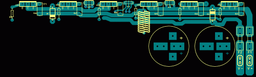
I too advocate the small loop area of the power input traces.
I add that the "Power" supply must include the Power Zero Volts.
The triplet of +ve, Zero Volts, -ve virtually cancel. Do this for both the twisted triplet power cable and for the paralleled traces on the PCB. And keep the Spkr output terminal very close to the power input triplet terminals, post74 shows this 4 terminal group.
Last edited:
I too advocate the small loop area of the power input traces.
I add that the "Power" supply must include the Power Zero Volts.
The triplet of +ve, Zero Volts, -ve virtually cancel. Do this for both the twisted triplet power cable and for the paralleled traces on the PCB. And keep the Spkr output terminal very close to the power input triplet terminals, post74 shows this 4 terminal group.
Your wish is my command .... ADCOM does it (below 1) , can't argue that fact. IN FACT , I always did agree that the science supports this as the optimum layout scheme. No argument there. So , this may take another few hours (Below 2) , but (small loop area , triplet , asymmetrical layout) will be the way.
Even as I thank Alex for that layout (post 74) , it is not applicable to the style that DIYA wants. Adcoms style is more in line with what is desired.
(almost)DONE - FIXED.
OS
Attachments
Yes and the MF & HF decoupling become much more effective.
The previous layout had an enormously long loop around the output devices and the HF decoupling ~500mm long.
I accept that DIYaudio guidance for a universal board will over-ride these layout ideas and I cannot and will not object if OST has to revert to previous to solve all the layout details.
Thanks to OST for all this great work.
Yes and the MF & HF decoupling become much more effective.
The previous layout had an enormously long loop around the output devices and the HF decoupling ~500mm long.
I accept that DIYaudio guidance for a universal board will over-ride these layout ideas and I cannot and will not object if OST has to revert to previous to solve all the layout details.
Thanks to OST for all this great work.
Thank you , for quieter amps
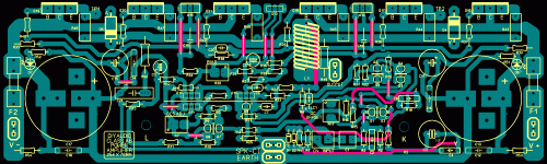
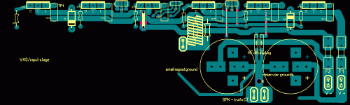
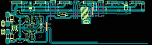
. Look below , would "K" as chassis ground be prudent coming into the main star. Note the 2 reservoir grounds and the small signal ground coming in from the left. Please comment on this.All are labeled (temporarily).
I can do this ... in fact, easily
Even keeping the "DIYA guidance" aspect. I want the best - any cost !PS - you can reach a screwdriver past the large caps to access the semi's now ...
OS
Attachments
Last edited:
The two reservoir grounds must be connected together before connecting to the Main Audio Ground (MAG).
The new layout will send a proportion of the cap charging pulses across the MAG and contaminate the spkr signal. If this on board reservoir is the sole smoothing after the rectifiers then this will be disastrous.
The new HF decoupling will be just as bad as the previous.
The HF decoupling must be located at the output devices and connect to each other via the shortest possible loop. That common Power Ground is then routed to the MAG.
The power should come into the fuses and go to the reservoirs. Then from the reservoirs to the Drain feeds. The reservoirs must not tap off the fuse to Drain feeds.
Do we really want/need the Thiele L//R on board?
Diodes from -ve to Zero Volts to +ve help prevent damage if the PSU is inverted. They also limit reverse voltage on the reservoirs to <=700mV if a fault develops that discharges one supply rail.
Are the two existing diodes the output to rail limiters? I note the connected one is rail to rail !
Last edited:
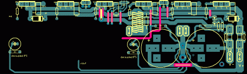
OK , I got it (below).
The small (HF decoupling) is after the fuse now (right to the rails / near OP's).
Show this concept - I might implement it, if small diodes (1a) can be used.
I need to change that to output/rail , it is a flyback diode - to keep back EMF from damaging the precious output stage .
OS
I looked at other Layouts and the big reservoir's have to be before the fuses. I charged my Altec 25Kuf capacitor bank through a 6A fuse , it only lasted for 3 inrushes (and deformed /melted). Smaller onboard decoupling (2 x 470-1kuf) can go after the fuse , but not the max 22Kuf that this board can accommodate. If that is what you really meant , sorry.The power should come into the fuses and go to the reservoirs.
The small (HF decoupling) is after the fuse now (right to the rails / near OP's).
Best to be fully self- contained (1 board) - 300 - 700$ to manufacture. If I keep the IPS far enough away , I'll be good.Do we really want/need the Thiele L//R on board?
Diodes from -ve to Zero Volts to +ve help prevent damage if the PSU is inverted. They also limit reverse voltage on the reservoirs to <=700mV if a fault develops that discharges one supply rail.
Show this concept - I might implement it, if small diodes (1a) can be used.
Are the two existing diodes the output to rail limiters? I note the connected one is rail to rail !
I need to change that to output/rail , it is a flyback diode - to keep back EMF from damaging the precious output stage
.OS
Attachments
what if the output coils and boucherot cells are located right at the speaker binding posts?
Just jumper the Inductor.
Some would not like this , so either way ... this is yet another OPTION. PS - the "construction/options" document is getting larger. OS
Look at this, (below) grounding/ rail config , it closely resembles the ADCOM , but has the big caps.
Attachments
1n4003 or higher will be just fine.
The two diodes from output to rails to catch that back EMF simply need to be repeated, but this time from Power Ground to rails.Since the rails and output and power ground are all near each other (for current field cancellation) all 4 diodes could be placed up between the power devices.
For big on board capacitance, I agree. The fuses, F type, must be after the main capacitance. That requires to power to be fed to the capacitors first and then to the fuses for onward supply to the rails. If you invert the main capacitance pair with it's Power Ground then the new location of the Power Ground is much closer to the Speaker output (and could be side by side). A pair of 1/4 blades could be positioned adjacent for a small loop area 4 way connection. It may be possible to combine blades within the footprint of a 4 way 16A insulated terminal block and leave access for cable entry and screwdriver tightening. I use either and am happy to see options to suit other builders.
Ahh, I see that post113 has shown the inverted caps and ground terminals.
Last edited:
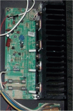
This project really has me jazzed. My Adcom GFA-535 has been with me for years and Anatech gave me some good advice in restoration of my amp.
OS, I recognize that Adcom board. It's from a 535, right?
This is the project I've been wanting to build for a long time! It will be way cool to put the amps side by side and listen.
OS, I recognize that Adcom board. It's from a 535, right?
This is the project I've been wanting to build for a long time! It will be way cool to put the amps side by side and listen.
1n4003 or higher will be just fine.
The two diodes from output to rails to catch that back EMF simply need to be repeated, but this time from Power Ground to rails.Since the rails and output and power ground are all near each other (for current field cancellation) all 4 diodes could be placed up between the power devices.
For big on board capacitance, I agree. The fuses, F type, must be after the main capacitance. That requires to power to be fed to the capacitors first and then to the fuses for onward supply to the rails. If you invert the main capacitance pair with it's Power Ground then the new location of the Power Ground is much closer to the Speaker output (and could be side by side). A pair of 1/4 blades could be positioned adjacent for a small loop area 4 way connection. It may be possible to combine blades within the footprint of a 4 way 16A insulated terminal block and leave access for cable entry and screwdriver tightening. I use either and am happy to see options to suit other builders.
Ahh, I see that post113 has shown the inverted caps and ground terminals.
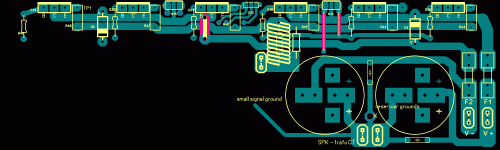
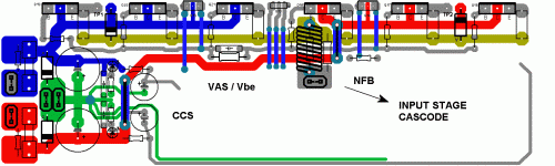
I decided on what is (below) for the current layout.
- Now it has "after the fuse" 470-1,000uf @63-80v standard main decoupling , followed by a 220-470uf secondary bank used for the R/C small signal filter/bypass.
- The 2 MUR320 (4003 ?) main decoupling diodes are in there ... this amp would be absolutely immune to reverse hookup.
- The V+/V- and OV(earth , ground) are close together now. No long runs of any return current pulses. The input stage ground and input stage positive rail will have to circle the bottom and right of the board , but they are 20mA - low current.
sonidos -This project really has me jazzed. My Adcom GFA-535 has been with me for years and Anatech gave me some good advice in restoration of my amp.
OS, I recognize that Adcom board. It's from a 535, right?
This is the project I've been wanting to build for a long time! It will be way cool to put the amps side by side and listen.
This is nearly the exact Adcom layout... yes , that is a 535/545.. The ADCOM has no onboard decoupling , no secondary filter/decoupling ... nothing !! The ADCOM is also a fully complimentary input stage , push pull VAS - EF2 (to fully describe it). ADCOM relies on the PSSR of the amp and 2 /4 "dirty" main caps to keep fidelity.
This DIYA amp is a bit more refined , with current sources and more decoupling. Power wise , like a 545.
OS
Attachments
Last edited:
That would bring us back to the symmetrical extended loop area we are trying to eliminate.
I still have the first artwork if VARIAC needs something quickly. I am busy integrating some of the excellent advice and ideas into this project. I aim to totally outclass ANY similar project with this one - DIYA /Ebay , or elsewhere.
I have all the classics , all the AB projects here at DIYA , and all that excellent advice.
I already have the VAS / ccs's / and input stage done one the first PCB , just click and past into the present one (with a few "tweaks").
Andrew's suggestion of the reduced loop area with no long patterns conducting high current pulses is the final factor which will make this the "Master" LIN amp. By keeping all that "dirty" current on one side of the layout will really make things "clean and quiet" on the input stage side.
At this point ,(below) I now have all 6 small decoupling caps , the zobel , and the input ground having a separate "starred" return which is also separate from the main caps and the speaker/OV spades. THIS is similar to the grounding scheme on the PCB of an AP AUDIO analyzer.
Should be good for a simple audio amp.
PS- I'm spending so much time on this because - 1. I am learning/researching , 2. This will be the same layout for my super - duper DBT/luxman triple OP amp. I WILL go "overkill" on both.
Attachments
- Home
- Amplifiers
- Solid State
- diyAB Amp - The "Honey Badger"