What is the relation between OLG phase and Output phase?
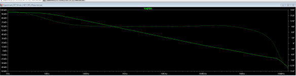
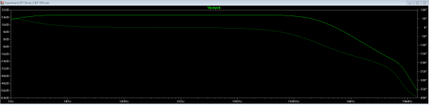
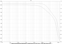
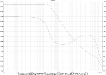
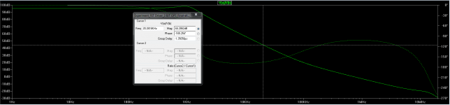
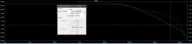
Doing some simulations of my amp and using the Audioamp.asc example in LTSpice shows the OLG and phase margin seen in the first picture, second picture shows output of my amp by AC analysis, with completely different phase and no phase margin whatsoever.
How important is the output phase, should there be some phase margin there as well?
Attachments
What is the relation between OLG phase and Output phase?
Doing some simulations of my amp and using the Audioamp.asc example in LTSpice shows the OLG and phase margin seen in the first picture, second picture shows output of my amp by AC analysis, with completely different phase and no phase margin whatsoever.
How important is the output phase, should there be some phase margin there as well?
Are both open loop?
jan didden
Are both open loop?
jan didden
No, the last one is just measuring the output of my amplifier using the AC Analysis in LTSpice. That should be closed loop.
I think your compensation needs work, the CL phase margin appears to be non-existent at gains and phase shift well above that required for oscillation. You really want about 60 degrees of margin at the 0dB intercept closed loop.
Introducing a first order roll-off (dominant pole) in the VAS at a couple of hundred kHz might do it, but without seeing the design it is hard to know.
Introducing a first order roll-off (dominant pole) in the VAS at a couple of hundred kHz might do it, but without seeing the design it is hard to know.
I think your compensation needs work, the CL phase margin appears to be non-existent at gains and phase shift well above that required for oscillation. You really want about 60 degrees of margin at the 0dB intercept closed loop.
Introducing a first order roll-off (dominant pole) in the VAS at a couple of hundred kHz might do it, but without seeing the design it is hard to know.
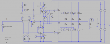
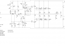
This schematic.
Everything is ok and simulates well, with low distortion, just need to do some work on the CL phase margin and Im done. But it turns out to be quite hard and I really dont know what to do about it.
Attachments
Your compensation network is undersized.
Increase C4 to 68pF, C8 to 270pf and R30 to 2.7K at least.
Im afraid it is not so simple, been playing around with different values for hours with no good result, OLG remains more or less excellent through it all with a phase margin of more than 60 degrees at all times. But the CL response is just crap no matter what combination I try. Offcourse I *CAN* get a good phase margin bur really destroys my THD-20, at 72 Volts peak-peak(around 80 Watt) and crap CL phase margin I get 0.003xx% THD, but with good phase margin(atleast 60 degrees) which requires some rather high cap values I get 0.05xx%
Try BJTS as drivers, as using mosfets at this place doesnt bring anything,
and often, quite the contrary.
Test with either MJE15032/15033 pair or 2SA1837/2SC4793 pair.
I wanted to isolate the VAS from the Output stage, hence the use of FET's as drivers.
I don't see how you measure OLG, v(a)/v(b). I can't find those on your schematic.
Could you attach LTspice files?
Because I have 2 schematic one for thd testing/other things and another for phase testing. Test phase in one, switch to other for thd testing. Then I only have to change each schematic a little.
Guess which schematic I posted.
")
If you want a help post LTspice files.
Well, here is the LTSpice file, but you might need some models, Im using Bob Cordells models when possible but the FET models are from Vishay(Irf).
.subckt files for the FET's are included in the zip.
Attachments
Last edited:
Here is simulation .ac result. It looks quite good for me. I changed TMC slightly.
For .ac OLG graf you have to take -V(a)/V(b), and I connected TMC resistor to the left side of the V6 to have TMC included in ac analisys. Phase margin is 70 degree, quite good.
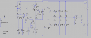
OLG, CLG and schematic attached.
For .tran sim I will need more time as I have to change simulation a bit more.
dado
For .ac OLG graf you have to take -V(a)/V(b), and I connected TMC resistor to the left side of the V6 to have TMC included in ac analisys. Phase margin is 70 degree, quite good.
OLG, CLG and schematic attached.
For .tran sim I will need more time as I have to change simulation a bit more.
dado
Attachments
Here is simulation .ac result. It looks quite good for me. I changed TMC slightly.
For .ac OLG graf you have to take -V(a)/V(b), and I connected TMC resistor to the left side of the V6 to have TMC included in ac analisys. Phase margin is 70 degree, quite good.
OLG, CLG and schematic attached.
For .tran sim I will need more time as I have to change simulation a bit more.
dado
So how did you do the ac analysis on CLG? What settings did you use?
So how did you do the ac analysis on CLG? What settings did you use?
Set V3 AC 1 and V6 AC 0.
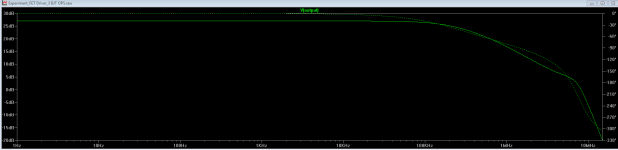
Well, did some more simulation, increased the LTP current from 1mA to 4.5 mA and adjusted the TMC cap values.
See attached schematic. Resulted in the attached OLG and CLG plots.
THD-1 with 1 Watt out into an 8 Ohm load gives 0.000004% distortion, rising to 0.000043% distortion at 60 Watt. THD-20 with 1 Watt out into an 8 Ohm load gives 0.000121% distortio,n rising to 0.004675% at 60 Watt.
Clipping occurs at somewhere between 80-90 Watt into an 8 Ohm load
Not the perfect amp but I'm quite happy about the results. Some tweaking will probably be required along the way to get optimum performance but as it is now it should give quite good performance.
Attachments
Last edited:
- Status
- This old topic is closed. If you want to reopen this topic, contact a moderator using the "Report Post" button.
- Home
- Amplifiers
- Solid State
- OLG Phase vs Output Phase