hm, you have hf switching hiss. it is -180db down @10MHz
in Kenpeter's proposition there is no HF hiss from >10KHz
but anyway I like you project very much")
I am pleased that you like it.
Any Way, i would like to see other versions of it and builds. It is not complicated to build also.
Hi Sonnya,
Your new design is very clever . . . not very high OLG but very low distortion.
My DC linked fetzilla version has higher OLG in the audio band which I'm enjoying very much just now but this upgraded version of yours is just too tempting to resist. It will be a good nice comparison of the different approaches.
I do enjoy high feedback amps if they're stable enough to also be smooth especially for classical music but I have the feeling your design is going to sound very good.
It may be a while before I will get around to it but I'll report here when I do
cheers
mike
Hi Mike.
The tested triple EF does not cause instability.
The only three reason to run it on a triple EF is:
The tested triple EF does not cause instability.
The only three reason to run it on a triple EF is:
- Less high order harmonics
- Easier to match than mosfets
- The Mosfet tested on my speakers and by Raidho on the C1 C2 and C3 gives a more soft bass section. We have not verified it but we think it is due to the fact that the rDS value raises with the increased Die temperature.
I would not inclined to add anything that causes stability issues so please excuse my ignorance but what is the advantage of adding a triple ef output stage ?
Hi Mike.
I am going to make a mosfet version of the AMP under All circumstances.
I Will let you know about the build.
Hi sonnya,
Yeah, I didn't really mean stability issues - just that the speed and stability of an amp is pretty high on my list priorities so I am disinclined to take designs in the other direction.
While doing spice research on DC linked fetzilla I found increasing the o/p stage bias was the simplest way to decrease high order harmonics and this slightly helps with stability. I have yet to do a real world comparison of different bias levels.
The levels of low order HD in this design are already so low that it is no longer an issue for me.
I also intend to build this design but to enable a direct comparison to other front ends I will use my composite Mosfet / Lateral mostfet darlington pair o/p devices.
Did you ever see an amp with mosfet / bjt composite darlington o/p devices ? I always thought this would be a pretty cool combination - but I never saw anyone do that.
cheers
mike
You have to draw this output stage. I cannot remember i have seen it.
The reason for the low distortion is the use of a driver stage for the mosfets.
You need to get rid of the gate charge and build it up fast. That requires a lot of current which the VAS stage cannot deliver.
I also discovered that standard current mirrors and folded cascode generates slewing related distortion. They both has to supply the compensation cap. And the output stage or the driver stage. The solution was to ADD current gain to the mirrors.
On the same time we need to raise the linearity of the mirror. That is the reason i have choosen Wilson current mirror.
The next problem was the fact that the current mirror with gain reducere the influence of the compensation cap by the gain factor.. We dont need more bandwitdh, just reducing the slewing distortion. So by applying the compensation cap across the current mirror fixed this problem.
I hope it explains how i Got there.
My o/p darlington pairs are shown in this thread here:
http://www.diyaudio.com/forums/soli...x-gain-mosfet-output-stage-7.html#post2775430
Only I use zvn & zvp3310a instead of 4424a
Better than VAS driving lateral mosfets direct - now VAS sees very small i/p capacitance of 3310a . . . .
Perhaps 10mA still too little current to drive laterals ?
but much lower op impedance than VAS
"laws of semiconductor physics" forever forbid complimentary jFETs.Without increasing costs...
Forget such designs.
Forget complementary Wilson current mirrors. Yo cannot get that working in practice.
Not Q1 throu Q6 sit on a thermally conductive plate held at constant temp. That is n-times better than "thermal compensation". Those who understand semiconductor physics understand immediately why this must be so.
Further Q7 Q10 must be mounted on a heatsink separate from the heatsink Q8 Q9.
Further Q7 Q10 must be mounted on a heatsink separate from the heatsink Q8 Q9.
"laws of semiconductor physics" forever forbid complimentary jFETs.
Forget such designs.
Forget complementary Wilson current mirrors. Yo cannot get that working in practice.
I do not fully follow you.
I think i have never spoken about complimentary JFET'S !? You can make a buffer with two N or P channel Jfets that will act like a complementary, but i don't think that this is what you mean.
For the record: Wilson current mirrors does work in practice.
But not complementary Wilson mirrors. of course one could select from a big bunch of devices those which yield a DYNAMICALLY (!!) complemnetry pair of Wilson mirrors but why? It is far more clever to follow a design rule that yields topologies insensitive to
such inevitable differences . Only ring-emitter or multi-emitter BJTs can be made dynamically complements, not simple Epi-planars. its not possible.
such inevitable differences . Only ring-emitter or multi-emitter BJTs can be made dynamically complements, not simple Epi-planars. its not possible.
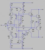
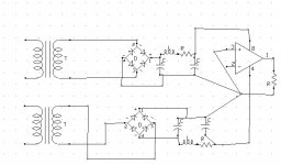
Power supply double star grounding
Hi Hafran,
You have not yet realised the full potential of having two separate secondaries & bridges in your PSU diagram.
Whether you use cheap noisy diodes of nice schhotky ones . . . when those diodes turn off a resonance will be excited in the secondary windings of the transformer - usually in the 1meg hz region.
In your diagram you are injecting that resonance directly into the amps earth - sonic disaster !
You need to either damp that resonance with a snubber cct or filter the earth lines before you make your star earth point - or do both !
- Status
- This old topic is closed. If you want to reopen this topic, contact a moderator using the "Report Post" button.
- Home
- Amplifiers
- Solid State
- Yet another amp - simple inverted with 10x gain, mosfet output stage