You are using an "inverted" logic compared to the Circlophone: detection of lack of quiescent current with subsequent ORing of + and - informations.. Some of the stoppers clearly are
not stopping much, and could go if the main
problem with stabilty was solved. It goes full
triangle by 40KHz, but even thats not got it...
Those Taylors are made not to ever shut off.
I don't know if thats part of the problem?
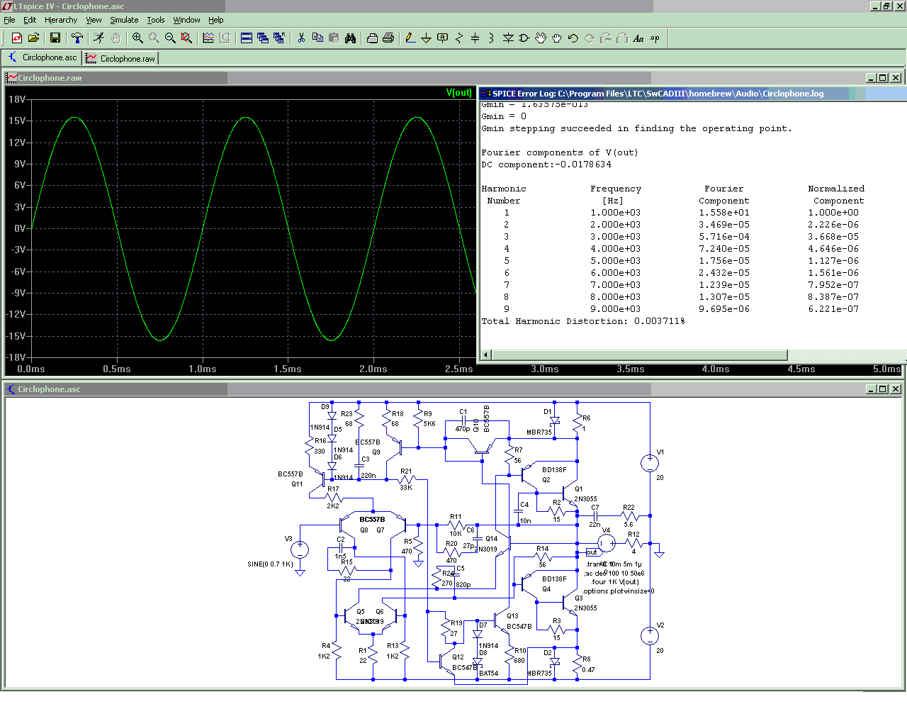
That's the path I tried to follow for months, when I was developing the Circlophone: it seemed natural and logical, and avoided the saturation issues of the other option.
I could arrive at extraordinarily good static or quasi static results, but the dynamic behavior was a nightmare.
In the end, I gave a try to the dual version, and miracle: the dynamic problems were gone.
There was a degradation in the static linearity, but it was acceptable, and the Circlophone was born.
Now, I am not saying all systems based on the lack of current are doomed, I have made successful attempts in the opposite direction, but for some reason I don't grasp, the "positive" variant seems more responsive
The stability margins of both loops seem rather marginal, some form of compensation would be needed to make the thing safe.Actually, a diode bridge between gates seems to fix the clipping instability.
Limits gate voltage difference to 1.4V, now hard clips and recovers clean.
Guess this also limits the maximum error stored in gate charges, thus the
quick recovery?
Still can't get this thing past 40K. If I ease up on comp, goes banannas.
Lessening the open loop gain helps stable bandwith, but hurts distortion.
Like for example: source resistors, or using a BJT limited by beta. Going
other way, to a MOSFET with even higher gain, stability is unobtanium.
Maybe I am pushing too few transistors for way too much open loop gain?
Feels like xquad again, though I doubt any negative resistance is at fault.
Interesting, but I fail to see the advantages of this configuration: ideally, we are looking for an optimum differential gain and linearity, and a minimal interaction between common and differential modes.And one more nutty unstable distraction for Elvee to ponder...
Same old same old, but new and improved with over and under.
Yeah verily, er whatever!
Evequad what I has in mind, more or less?
Anyways, yes it works. No, not any better.
This might have been worth exploring, but
I am ready to concede it is not fully baked.
Weird thing here: Gain is max when emitter
resistors (and diodes) are abused up top, to
match the ones on the bottom. Not just the
distortion goes down, open gain goes up!!!
Bigger or smaller resistors lose gain, why?
But open loop gain here is not comparable
to a plain old xquad, nor even the CFP way.
This Evequad seems only just barely gainful
enough to get the open loop job done, and
I don't really understand it well enough to
know what stability means in this contex.
Attachments
Last edited:
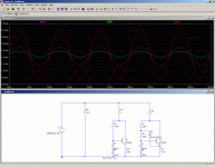
Bandwidth is up, and behaving well for both reasonable
(soft clipped) and unreasonable (hard clipped) overloads
at the input. Both input transistors stay on til the clipping
nonsense gets way beyond even that...
I was just trying to keep these transistors on, when I
noticed a problem with diodes from input to output...
If you don't attenuate that feedback, it can be mis-
interpreted as a positive and aggravate the clipping,
maybe even latch.... Give it anything less than unity,
and the problem does not occur.
So basically, anytime the output can't properly follow
the input, the input is attenuated to a smaller copy of
the distorted output. Prevents all sorts of wacky evils
when faced with the impossible.
Thats when I got this dumb flash that maybe this is
also where my comp should go? YESSS.... that worked!
Finally could loosen the screw on those output transistors.
40KHz lookin' siney with just a little bit of triangle, and
tips not bent (phase shifted?) too much forward nor back.
Attachments
More foolishness from the same bag...
Drop either rail to 12V and watch it shut off.
---
Do you ever get the impression that an amplifier
trying to play music is like a guy at the hardware
store trying to juggle an egg with vice grip pliers?
Drop either rail to 12V and watch it shut off.
---
Do you ever get the impression that an amplifier
trying to play music is like a guy at the hardware
store trying to juggle an egg with vice grip pliers?
Attachments
Last edited:
I powered up new pcb but it shows 300mV level dc-offset. If I bypass input cap and shortcut input to ground, It is falling to 50mV level and decreasing to 1mV slowly in a minute. But starting to increase again just after. I have no idea where to look at. Any advice please?
Last edited:
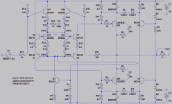
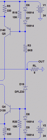
Looks to me: 7V too much Zener, or 7V too little power supply?
You could try a cascode at output potential, rather than a zener.
Q5 Q6 won't have any excuse to see different collector voltage.
D10 or D11 might be faulty?
One of your thresholds is maybe higher than the other?
Why is there only .1V drop across Q7?
You could try a cascode at output potential, rather than a zener.
Q5 Q6 won't have any excuse to see different collector voltage.
D10 or D11 might be faulty?
One of your thresholds is maybe higher than the other?
Why is there only .1V drop across Q7?
Last edited:
D10 or D11 might be faulty?
Spot on!
Thank you Ken, after replacing D10-11 it seems it is ok now. Let me see how it performs.
Looks to me: 7V too much Zener, or 7V too little power supply?
You could try a cascode at output potential, rather than a zener.
Q5 Q6 won't have any excuse to see different collector voltage.
My previous builds were having same issue and Elvee told me that it is not possible everytime to getting exactly half of the total supply voltage with zeners. This voltage difference doesn't affect sonic performance of amplifier according to him, if I remember correctly. If you can find an opportunity, it may involve us if you clarify with some schematic that what you mean with "cascode at output potential, rather than a zener".
Regards.
Last edited:
After removing light bulb from mains, Q5's collector voltage measured as ~ -1.5V (Q6 is -0.65V). It seems voltage drop caused by light bulb produced measurements on picture. I was realised that I have to use total 30V zener with my 31V supplies when using 2x16V at previous builds. Then I switched to single 30V/1W.
Elvee: You specified Q5 and Q6 as 2Vs, but I can't see any voltage gap greater than Vs on their legs. All measurements are negative. I'm asking this because I want give a try Philips BD137's as Q5/Q6 with my 31V supplies.
Elvee: You specified Q5 and Q6 as 2Vs, but I can't see any voltage gap greater than Vs on their legs. All measurements are negative. I'm asking this because I want give a try Philips BD137's as Q5/Q6 with my 31V supplies.
Last edited:
Here is the cascode version.If you can find an opportunity, it may involve us if you clarify with some schematic that what you mean with "cascode at output potential, rather than a zener".
It has not been physically tested, just simmed, but it should work without problem.
During the positive excursions, Q6 sees up to ~2*Vs Vce. And since Q5 has to be identical to Q6, both need the 2*Vs voltage rating.Elvee: You specified Q5 and Q6 as 2Vs, but I can't see any voltage gap greater than Vs on their legs. All measurements are negative. I'm asking this because I want give a try Philips BD137's as Q5/Q6 with my 31V supplies.
In principle, you could also try small MOSfets for Q5 and Q6. Small, low capacitance types like BSS145 should be suitable.
R6 and R7 would have to be increased to ~2.7K.
This has not been tested either.
Attachments
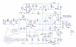
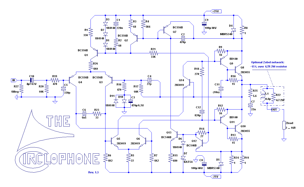
And, so does the RC, R18-C12 go on the phase inverter side as shown in this simulation?:
http://www.diyaudio.com/forums/atta...little-cheap-circlophone-circlophonekpmod.gif
Or, does it go on the driver side as shown in this picture?:
http://www.diyaudio.com/forums/atta...little-cheap-circlophone-thecirclophone13.gif
P.S.
Maybe I need to redo my layout to put the phase inverter (and input pair) at 1cm or less distance from the drivers? That would relocate Q2/Q7, Q12/Q13 to the opposite end of the board from the drivers. However, that layout change would make the feedback and phase inverter connections direct rather than jumpered. Some of the PCB examples also show jumpers or long distance connection via circuitous traces taking the scenic route. Does that section need flipped? Turning it over makes the signal caps and input cable arrive at the center of the board which is the trade-off for not jumpering phase inverter and feedback.
That's the correct versionOr, does it go on the driver side as shown in this picture?:
http://www.diyaudio.com/forums/atta...little-cheap-circlophone-thecirclophone13.gif
That aspect is completely irrelevant here, this is low to medium signal level, and more importantly, it operates in current-mode, making the signal practically immune to track lengths or contortions.Maybe I need to redo my layout to put the phase inverter (and input pair) at 1cm or less distance from the drivers? That would relocate Q2/Q7, Q12/Q13 to the opposite end of the board from the drivers. However, that layout change would make the feedback and phase inverter connections direct rather than jumpered.
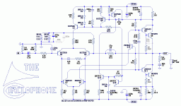
Here is post 1 schematic altered to modular. That took all day. I hope its right, but it needs checked out.
I also tried to decrease the occurrence of subharmonics or spurious noise causing D10, D11 misfiring by, instead, passing larger signals through a larger capacitor as needed and by doubling the switch on voltage of the diodes. There is also signal star ground arrangement in that it visually appears closer to a balanced amp. I hope this is okay.
Instead of showing a sky high gain, I decreased the operating voltage; so, now a computer might be able to push this to potential. It has about the same operating voltage as post 1 and the same gain setting. It also has a 3055, but this time, its TIP3055, supposedly the same (except PD), but it fits the PCB designs.
An additional protection that could be very useful is a diode clipper at input because, especially computers, random sources are prone to emit a spike or surge, especially at power up or power down, and this also happens if using a source selector dial. I didn't know exactly how to add the diode clipper, but would like to know.
Q14 is shown. I hope I got everything shown correctly this time. It should render tack sharp 1024x600, which fits the entire schematic onto the screen of any computer, including a netbook. There is no footnote for R21 but I was wondering if it is possible to, perhaps, use a transistor or two to facilitate wide voltage tolerances instead of changing the resistor? If not, then there is room for a handy little chart added later.
Attachments
Due to my location's terrific ambient RFI noise, I was in struggle by efforts of "dead silence" achievement again as like as my -blown- very first build. But it didn't happen again. I haven't any serious issue with my second build which was a powerflux pcb layout. It is comfortably silent but not "dead" obviously. I'm sure that there is something special with this topology which gains such silence but it seems I have to live with my ambient RFI noise at low levels.
Elvee: Regarding to post #261, should I use equal volume pot each side or implementation permits just one pot at positive side?
Elvee: Regarding to post #261, should I use equal volume pot each side or implementation permits just one pot at positive side?
I suspect shutdown of transistors and/or diodes in the quadrature loop
breaks up oscillation and squelches noise in the main loop... If you run
the quadrature loop in a shutdown-proof way too, things can get ugly.
This amp also runs at absurdly low quiescent current, considering the
smoothness of its crossing. Elvee also did his homework on PSRR.
breaks up oscillation and squelches noise in the main loop... If you run
the quadrature loop in a shutdown-proof way too, things can get ugly.
This amp also runs at absurdly low quiescent current, considering the
smoothness of its crossing. Elvee also did his homework on PSRR.
Last edited:
I do not exactly see what you mean, but there is no way the diodes could "misfire" or generate spurious noise: even when the amp is reproducing a full power 10Hz signal, the voltage seen by the diodes remains lower than 100mV, and even schottky's wouldn't have a chance to begin conducting under those conditions.I also tried to decrease the occurrence of subharmonics or spurious noise causing D10, D11 misfiring by, instead, passing larger signals through a larger capacitor as needed and by doubling the switch on voltage of the diodes.
The diodes only role is as a safeguard, in case something goes wrong with the supplies powering sequence for example, to avoid excessive charge building up on C3.
Doubling them means the output voltage during unexpected transient conditions could practically reach the supply rails, which is undesirable and will almost cancel their usefulness.
No problem with that.There is also signal star ground arrangement in that it visually appears closer to a balanced amp. I hope this is okay.
A good clipper could be nice, but unfortunately, any simple scheme operating at a meaningfully low level will have an effect on linearity.An additional protection that could be very useful is a diode clipper at input because, especially computers, random sources are prone to emit a spike or surge, especially at power up or power down, and this also happens if using a source selector dial. I didn't know exactly how to add the diode clipper, but would like to know.
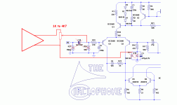
To avoid very severe spikes damaging the B-E junctions of Q4 and Q3, one could add a pair of back to back diodes between the bases.
This will not actually clip anything, but it will not impact the linearity, and it will make the input practically bullet-proof.
Note that the clipping of the amplifier itself is clean. It is hard, of course, but clean. Any soft-clipping scheme will have to eat up some of the output dynamic.
Q14 is basically identical to Q5 and Q6: same operating voltages and currents, same dissipation.Q14 is shown. I hope I got everything shown correctly this time. It should render tack sharp 1024x600, which fits the entire schematic onto the screen of any computer, including a netbook. There is no footnote for R21 but I was wondering if it is possible to, perhaps, use a transistor or two to facilitate wide voltage tolerances instead of changing the resistor? If not, then there is room for a handy little chart added later
A two-wire, 1.5mA current source could be substituted for R21. I have described some two transistors examples here and here.
Here, only a very crude accuracy is required, and a single transistor with two diodes or one LED would be sufficient.
Very strange.....Due to my location's terrific ambient RFI noise, I was in struggle by efforts of "dead silence" achievement again as like as my -blown- very first build. But it didn't happen again.
Here is a possibility, but the differential offset of your source has to be ~0 (ideally a transformer) to be able to do that.Elvee: Regarding to post #261, should I use equal volume pot each side or implementation permits just one pot at positive side?
A better option is to locate the volume pot upstream, at a place where the signal is in unbalanced form.
Attachments
Last edited:
Here is a possibility, but the differential offset of your source has to be ~0 (ideally a transformer) to be able to do that.
A better option is to locate the volume pot upstream, at a place where the signal is in unbalanced form.
I did it very quick and dirty way with two different pcb's. Either suffered serious dc-offset problem which is not a case of connect a speaker. If source connected, dc-offset beginning from five hundreds of mV then rises up to many volts step by step. I source not connected, i see at least 10 Volts for first. I'm not about to find a immediate solution, just bringing news of what happened. My source is a voltage-out dac chip's differential analogue output pins. I used 5K pot. Probably my source is not suitable for doing such thing.
Last edited:
- Home
- Amplifiers
- Solid State
- ♫♪ My little cheap Circlophone© ♫♪