I hope to make a discrete amplifier some day soon. This design has peaked my interest. Aprox 15 CAD of silicon per channel and a forgiveness of build quality and part selection make this very interesting.
I have a few questions, some of them smarter then others:
1- Would a pair of MJE3055T work for power transistors? I ask because Heat sinks for TO-220 are easier to build. (I suspect the answer is "yes, but only for less then 20v rails")
2- Does the PSU need anything more fancy then transformer, rectifier bridge and caps?
3- (The newbie question) how does one turn the PNG that powerflux posted into a PCB. More to the point, how does one extract the bits that are copper and print that at the right scale? I gave a stab in the GIMP selecting various bits by colour, filling with white or black, but this seems ackward. What's more how do I get the scale exactly right? Powerflux hasn't posted dimensions.
I plan to do the laser-toner-flimsy-paper-iron-on transfer method for creating the PCB.
I built with MJW21196 outputs (6 mhz to3p) and b649 drivers. Also used +-40v rails. Psu was toroid + 7*2200uf per rail, crc, shared both channels. Used "stealth" (fast and soft recovery) diodes.
Before final assembly though, the test supply was lacking: 1000uf per rail and a very undersized transformer. sound was better with better supply, obviously more audible at loud volumes. I was surprised at how well it sounded with the poor supply though.
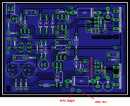
The PCB I used was made into a pdf easily printable a few pages back, by me. I used 100nf to bypass the electrolytics on the supply rails, soldered under board. The PCB does have one trivial mistake, incredibly easy to fix, that was also written about recently.
You will have to wait Powerflux is satisfied enough with his work to post the source file and/or a printable file.
I just hope he wasn't put off by my comments, that was only constructive criticism, and I appreciate any contribution, including his....
not put off at all
") just very busy. hopefully tomorrow. rerouting feedback combined with a proper central groundplane (most important updates) is time-consuming. i like the PCB to be 'Elvee'-approved and the schematic to be well-readable before posting eagle pcb files to prevent wild growth.
just very busy. hopefully tomorrow. rerouting feedback combined with a proper central groundplane (most important updates) is time-consuming. i like the PCB to be 'Elvee'-approved and the schematic to be well-readable before posting eagle pcb files to prevent wild growth.
Last edited:
new pcb. (v0.3)
fixed
- feedback
- central ground plane
- replaced ground connector. i'd star-ground everything at the main psu, that's why i decided to put it there.
i can't fit decoupling capacitors in the current version. The caps are either too small and other traces have to be rerouted to far away to connect them properly, or too large and thus don't fit on the board.
what i would do is simply 'free wire' the caps. that way you can place them directly
where you want to.
havent updated the schematic yet.
i want to wait until Elvee approves, then i will post a pdf or the files. for the people who cannot wait: the resolution is 300dpi, good luck
possible upgrades
- space for cooling fins for drivers
- minor adjustments input stage routing
fixed
- feedback
- central ground plane
- replaced ground connector. i'd star-ground everything at the main psu, that's why i decided to put it there.
i can't fit decoupling capacitors in the current version. The caps are either too small and other traces have to be rerouted to far away to connect them properly, or too large and thus don't fit on the board.
what i would do is simply 'free wire' the caps. that way you can place them directly
where you want to.
havent updated the schematic yet.
An externally hosted image should be here but it was not working when we last tested it.
i want to wait until Elvee approves, then i will post a pdf or the files. for the people who cannot wait: the resolution is 300dpi, good luck
possible upgrades
- space for cooling fins for drivers
- minor adjustments input stage routing
Last edited:
v0.4, small adjustments. just printed it on A4 to see it in real life, see attached PDF. it is tiny

comments? i'm not sure about the return currents in some places, wich is the big disadvantage of a continuous groundplane.
keeps the etching-liquid clean tough and more serious: there isn't much current to return through the plane where the traces are small. all the relevant ground stuff is happening on the left side, where the plane is decent.
comments? i'm not sure about the return currents in some places, wich is the big disadvantage of a continuous groundplane.
keeps the etching-liquid clean tough
and more serious: there isn't much current to return through the plane where the traces are small. all the relevant ground stuff is happening on the left side, where the plane is decent.Attachments
Last edited:
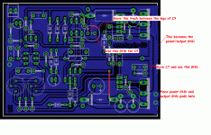
The input is in the right region regarding the ground.
To avoid passing high currents at unpredictable places of the ground plane, I suggest you set the position of the supply (power) ground and output ground pads.
Placing them in proximity will avoid uncontrolled dispersion elsewhere.
Note:
By pushing the diodes towards the center of the board, there would be room enough for decouplings.
Attachments
Elvee & Kenpeter, would like to thank you both for an hour or more of very interesting reading... my small mouse infested brain is spinning in quadrature loops I am certain... fun.
The resistor comment I made months ago referred to what I have subjectively found for years and is apparently backed up by Simon's post (and off forum tests) in the John Curl Blowtorch thread.
But the best post was Elvee's on the effect of layout vs. real world performance! Nice.
_-_-bear
The resistor comment I made months ago referred to what I have subjectively found for years and is apparently backed up by Simon's post (and off forum tests) in the John Curl Blowtorch thread.
But the best post was Elvee's on the effect of layout vs. real world performance! Nice.
_-_-bear
The input is in the right region regarding the ground.
To avoid passing high currents at unpredictable places of the ground plane, I suggest you set the position of the supply (power) ground and output ground pads.
Placing them in proximity will avoid uncontrolled dispersion elsewhere.
Note:
By pushing the diodes towards the center of the board, there would be room enough for decouplings.
why not put the output ground with the supply ground at the main capacitors (star ground)? that way the return current of the output stage won't even go through the PCB.
It is an option, but then you cannot use local (free wire) decoupling caps, because they will "pollute" the local ground by injecting class B waveforms from the supply rails.why not put the output ground with the supply ground at the main capacitors (star ground)? that way the return current of the output stage won't even go through the PCB.
And anyway, a pad costs nothing, so why exclude that option?
like this? i really dislike the way the drivers are routed. there is only space for the tiniest decoupling caps..
An externally hosted image should be here but it was not working when we last tested it.
Last edited:
I am not too concerned about the drivers, but the way C9 returns to the ground is a problem: it loops back more or less randomly through the input section, and this is going to cause troubles.like this? i really dislike the way the drivers are routed. there is only space for the tiniest decoupling caps..

The best solution would be to push the big schottky's D4 & 5 towards the center of the board and place the decouplings on the outside, near the edges.
Alternatively, as a second best, it is possible to choose a better return path for C9, without modifying the placement of components.
See pic.
It is also important to define a power and output ground clearly, where the Zobel also has to return: mainly to the right of the board.
Attachments
Member
Joined 2009
Paid Member
... I hear the Circlophone, and I have more detail in the music than I have ever heard, and I am talking about songs I have been listening to since I was a kid. On top of that it is so musical and "sweet" than I always want to switch it on and play music, even in the most inappropriate situations.
This is a great endorsement - and I remain attracted to the sheer ingenuity of this design. My 2N3055's are still waiting unused for me to finish other projects but I shall be keeping an eye on this Circlophone
i'll just enlarge the PCB a bit, that's the best way to fix these issues
Hi powerflux,
I really appreciate your effort on this circuit..any update of your pcb layout? Thank you..
Regards,
Boyet
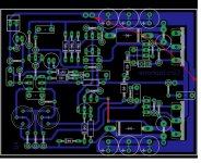
a quick one. forgot about this project since i'm buisy with an I/V converter.
let's call this 0.6.
- enlarged PCB a bit
- fitted caps
now i want to get rid of the whole groundplane on the left side and just route on specified path back. opinions?
EDIT: like this. 0.7
let's call this 0.6.
- enlarged PCB a bit
- fitted caps
An externally hosted image should be here but it was not working when we last tested it.
now i want to get rid of the whole groundplane on the left side and just route on specified path back. opinions?
EDIT: like this. 0.7
An externally hosted image should be here but it was not working when we last tested it.
Last edited:

This time, I think it is about OK. I would just change the placement of the power and output ground pads to eliminate the effect of the class B current from the positive side, but otherwise it is good, and this applies to all versions.
The ones with the complete ground plane are more risky, less deterministic: they might very well outperform the plain boring single ground ones, but I cannot tell for sure.
Any version will perform acceptably.
Some refinements would still be possible to minimize induction effects from the outputs currents, but the improvements gained would be below the current level of performance of the amplifier, and a proper dressing/placement of the wiring would give similar results so I think we can leave it there.
Attachments
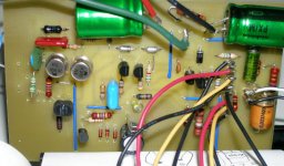
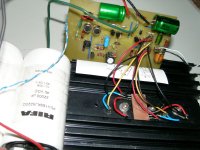
My dirty setup
At last I finished and listened one channel. I have modified wakibaki's pcb respecting 2sa/2sc small signal transistors. During populating parts, it was not easy to deal with narrow headers and bridges.. just needed some patient.
My setup:
2sa970 as PNP small signal
2sc2240 as NPN small signal
2sa1930 as Driver
2N3442 as output (test setup)
2N3020 as bias servo
180pF as C12 (servo compensation)
1200pF as C6 (main compensation)
31V per rail
Unbalanced signal
After sure that there is nothing wrong with dc-offset, bias current etc, I plugged speakers. On first listen, I realized that all efforts was absolutely worthy for this amazing amp! I'm listening one channel with two speakers parallel and I'm forgetting each time that I'm listening actually one channel.
First big impression is DEAD SILENCE even with my 100db speakers! I never expected this level of silence. There are radio station antennas near my house those interfere with my gear easily. Circlophone barely kicked it.
Second big impression is human voice. Just impressive!
Detailed, well bodied presentation without any haze as mentioned by oddyseybmx before. I gained my expectations so far and I hope to finish second channel in short time.
Thank you for all collaboration.
Attachments
Last edited:
- Home
- Amplifiers
- Solid State
- ♫♪ My little cheap Circlophone© ♫♪