Elvee:
I looked for it in all these posts (179, I almost went blind), but could not find it:
The Circlophone produces about 20+ watts as shown in the current schematic. Changing the output power requires what changes to the circuit? I believe 25/50/100 watt versions would be of interest to the Circlophonites. Could you post suggestions to the parts value changes?
Thanks, E
I'm using about +-40V and I only had to change value of R21 and use higher Vceo for two small signal transistors. Others may have to use something other than BD139/40 And depending on the output transistors, use more of them.
I'm not sure of the power capabilities of mine but it is more than sufficient. I'm moving and have been packing and cleaning with it cranked right up.
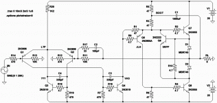
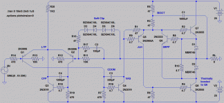
The output power is related to the supply voltages and the load impedance, in this case:Elvee:
I looked for it in all these posts (179, I almost went blind), but could not find it:
The Circlophone produces about 20+ watts as shown in the current schematic. Changing the output power requires what changes to the circuit? I believe 25/50/100 watt versions would be of interest to the Circlophonites. Could you post suggestions to the parts value changes?
Thanks, E
Po=(Vs-1.5)²/(2*Rload)
With the 25V supplies of the example, this translates into ~34W on 8Ω, ~30W for practical purposes, 60W on 4Ω, 120W on 2Ω and 15W on 16Ω
- For 8Ω:
Po=25W Vs=22V R21=33K
Po=50W Vs=31V R21=47K
Po=100W Vs=42V R21=68K
- For 4Ω:
Po=25W Vs=17V R21=22K
Po=50W Vs=23V R21=33K
Po=100W Vs=32V R21=47K
All small signal transistors except Q13 must have a Vceo>Vs, all the other, including Q13 must have a Vceo>2*Vs.
The combination of output transistors + heatsink must be able to dissipate ~Po/2 with an acceptable temperature rise.
For the lowest power levels, account must be taken of the quiescent power, which is higher than for a standard class AB: ~200mA.
That translates into heatsinks of 9°C/W for 10W, and 1.5°C/W for 100W for example.
At higher power level, the SOAR of the transistors will be the limiting factor, rather than Pdmax or Rth.
I'm using about +-40V and I only had to change value of R21 and use higher Vceo for two small signal transistors. Others may have to use something other than BD139/40 And depending on the output transistors, use more of them
That's about 90W for 8Ω
Single ended with the offset correction of an LTP:
Q2 is in a CFP, and operates at constant current.
Q1 sees low impedance tail strongly following Q2.
Q1 gets full amplification rather than usual half...
Q1 and Q2 balance at same current and voltage.
Go figure...
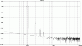
FFT shown at 1W 1KHz
Q2 is in a CFP, and operates at constant current.
Q1 sees low impedance tail strongly following Q2.
Q1 gets full amplification rather than usual half...
Q1 and Q2 balance at same current and voltage.
Go figure...
FFT shown at 1W 1KHz
Attachments
Last edited:
You see, I was screwin' with dis here one armed LTP.
Frustrated that currents did not automagically balance.
Something should be able to modulate the tail to fix that.
Now Q2 is held constant current by R19 and CFP loop.
Q1 is held similar average current by R7 and Noble loop.
Single ended result was complete unexpected accident.
Unexpected too was doubling of Q1's gain, probably why
the closed loop distortion went down so much as it did..
Was at least 10db worse H2 H3 before this new circle
began chasing its own tail.
C4 might not be needed. I just stuck it there cause it
looked "symmetrical". No thought process involved.
Last edited:
Member
Joined 2009
Paid Member

Whoa, thats weeeerd. C4 might be essential!
ACurrents in Q2 are much smaller than Q1 as expected, but phase shifted.
Wasn't planning, didn't want, and who invited a phase shift to this party?
I think this might be caused by compensation cap C3 in the Noble loop.
C4 definitely works to re-align push and pull phases in the LTP.
Aligns best at some value between 1200pf-1500pf, much higher than C3!?!
But why should this value be any different than C3? I don't get it...
---------
OK, I get it now... C3 sees VAS swing (Miller), C4 sees far less movement.
Last edited:
Messin to find ideal comp and junk... This 1W after reducing C2 to 33pF.
I'm guessin soft clip Zeners in parallel must have added a few picos?
Harmonic Frequency Fourier Normalized Phase Normalized
Number [Hz] Component Component [degree] Phase [deg]
1 1.000e+03 4.040e+00 1.000e+00 -0.26° 0.00°
2 2.000e+03 4.856e-05 1.202e-05 -104.81° -104.55°
3 3.000e+03 9.788e-06 2.423e-06 2.27° 2.53°
4 4.000e+03 1.788e-07 4.425e-08 149.89° 150.15°
5 5.000e+03 6.531e-06 1.616e-06 179.04° 179.30°
6 6.000e+03 1.198e-07 2.965e-08 161.53° 161.79°
7 7.000e+03 4.024e-06 9.959e-07 -1.21° -0.96°
8 8.000e+03 7.927e-08 1.962e-08 -161.45° -161.19°
9 9.000e+03 2.339e-06 5.790e-07 178.96° 179.22°
Total Harmonic Distortion: 0.001242%
And this at +/-19.5V peaks, just under threshold of soft clipping:
Harmonic Frequency Fourier Normalized Phase Normalized
Number [Hz] Component Component [degree] Phase [deg]
1 1.000e+03 1.914e+01 1.000e+00 -0.22° 0.00°
2 2.000e+03 1.367e-03 7.143e-05 -101.98° -101.75°
3 3.000e+03 8.989e-04 4.697e-05 3.44° 3.66°
4 4.000e+03 7.046e-05 3.682e-06 85.50° 85.72°
5 5.000e+03 6.071e-04 3.172e-05 178.42° 178.64°
6 6.000e+03 6.539e-06 3.417e-07 56.44° 56.66°
7 7.000e+03 4.896e-04 2.558e-05 -2.90° -2.68°
8 8.000e+03 3.884e-06 2.030e-07 -108.80° -108.58°
9 9.000e+03 3.726e-04 1.947e-05 176.43° 176.65°
Total Harmonic Distortion: 0.009676%
And C4 is 1000pf right now too. Allowin' just a little shift seemed to
reduce simulated distortion. Again, its a mystery to me why a phase
shift across the LTP would do anything beneficial???
Last edited:
Needs... more... circles...Like a hole in the head.
Dear all,
 please remind me how to use asc file to get from it working schematic in ltspice, my ltspice reads it as txt file
Last edited:
You right-click on it, choose "save as", and edit out the .txt (one of many methods possible).Dear all,
please remind me how to use asc file to get from it working schematic in ltspice, my ltspice reads it as txt file
.Single ended with the offset correction of an LTP:
Q2 is in a CFP, and operates at constant current.
Q1 sees low impedance tail strongly following Q2.
Q1 gets full amplification rather than usual half...
Q1 and Q2 balance at same current and voltage
Clever scheme.
I find that C4 can be removed completely.
If you want to go even further in that direction (linearizing the LTP), another method is to use a crossquad.
The beast is difficult to tame, but it's worth the trouble:
THD @1W 1KHz can easily be pushed deep below the ppm threshold
Other than thermal backbond and fuses, can't figure a benign
way to soft limit current into a shorted load.
That wouldn't be very difficult by inserting current-sensing resistors in the supplies of the output stage, and it would interfere very little with the normal functionning of the amp.
Attachments
Last edited:
You right-click on it, choose "save as", and edit out the .txt (one of many methods possible).
...cannot make this in Win7,
txt extension cannot be deleted...
Then save it complete with the .txt extension, and the come back to it, and edit the filename to remove the .txt.
...cannot make this in Win7,
txt extension cannot be deleted...
Then save it complete with the .txt extension, and the come back to it, and edit the filename to remove the .txt.
as above,
cannot make this...
there is no txt extension in the name, but the file has txt in the properties...
in XP I was able to make it, but under Vista or W7 impossible... or I do not know how...
I will try to make this in win commander or similar,
thanks
PS Total commander has option to change the extension, I solved the problem, sorry for offtopic
Last edited:
i've read the whole topic but i feel like i still missing something.
what about the thermal effects and biasing? normally, the biasing transistor and/or diodes or whatever should be on the same heatsink as the output BJT's. in the PCB layout posted before they weren't even close.
maybe i don't understand the circuit correctly (i'm fine with the other claims, there are more simple amplifiers like the ESP P3a that don't need matching or adjustment to work forever), but how does this stay thermally stable?
what about the thermal effects and biasing? normally, the biasing transistor and/or diodes or whatever should be on the same heatsink as the output BJT's. in the PCB layout posted before they weren't even close.
requires no adjustment, no matching, no thermal compensation and yet has a rock-solid thermal stability
maybe i don't understand the circuit correctly (i'm fine with the other claims, there are more simple amplifiers like the ESP P3a that don't need matching or adjustment to work forever), but how does this stay thermally stable?
Last edited:
You are indeed missing something: the whole point of the Circlophone topology is the complete riddance of thermal problems, compensation, etc:i've read the whole topic but i feel like i still missing something.
what about the thermal effects and biasing? normally, the biasing transistor and/or diodes or whatever should be on the same heatsink as the output BJT's. in the PCB layout posted before they weren't even close.
maybe i don't understand the circuit correctly, but how does this stay thermally stable?
The servo stabilizes the quiescent current, but it goes further: it actively controls the output stage so that both sides always remain active in a "warm" class AB, having most of the attributes of the full class A, including a complete absence of crossover artifacts.
It is extremely easy to build, offers excellent performance even with 2N3055's, requires no adjustment, no matching, no thermal compensation and yet has a rock-solid thermal stability.
The circuit is completely under servo control, thanks to the current-sensing resistors, R8 and R11 and their associated circuitry.
The servoing action controls the quiescent current, without needing such messy things as Vbe multpliers or adjustable resistors, but it also goes further, and forces the output stage to remain in class A under large signal conditions.
Which demonstrates the concept does indeed work as advertised: ask odysseybmxin the PCB layout posted before they weren't even close.
The circuit is completely under servo control, thanks to the current-sensing resistors, R8 and R11 and their associated circuitry.
The servoing action controls the quiescent current, without needing such messy things as Vbe multpliers or adjustable resistors, but it also goes further, and forces the output stage to remain in class A under large signal conditions.
i understand now, i missed what to look for. the 'servo' is quite big (relative to the rest)
")
thank you. i will build this amp in the following weeks. i've got a +/-32V SMPS from a Linn integrated system that has been lying around for months waiting for something interesting; and that has just been found
i've read the whole topic but i feel like i still missing something.
what about the thermal effects and biasing? normally, the biasing transistor and/or diodes or whatever should be on the same heatsink as the output BJT's. in the PCB layout posted before they weren't even close.
maybe i don't understand the circuit correctly (i'm fine with the other claims, there are more simple amplifiers like the ESP P3a that don't need matching or adjustment to work forever), but how does this stay thermally stable?
In my case: the SRPP biasing transistor should be on same sink as close
to Q8 as possible. Q8 gets a little hotter than its mate because it gets
no help from base to emitter current leak. Schottky diode stack should
mount to a separate sink. When SRPP transistor gets heated, but diode
voltage drops are cooler ambient, bias is shunted away from JLH splitter.
Total bias available for sharing by both output transistors is modulated.
This is where it behaves like the circlophone, yet completely different.
I would bolt collector of hottest transistor Q8 directly to live sink, with
no electrical insulating pad, only grease. Q6 and Q7 would require pads.
If you prefer to drill a TO-18 hole and stuff Q6 into it, then I guess Q8
would need a pad too. Only one transistor can be in direct contact....
Last edited:
If you want to go even further in that direction (linearizing the LTP), another method is to use a crossquad.
The beast is difficult to tame, but it's worth the trouble:
THD @1W 1KHz can easily be pushed deep below the ppm threshold
unbeliavle how important are inductors and 1.5 ohm resistors
- Home
- Amplifiers
- Solid State
- ♫♪ My little cheap Circlophone© ♫♪