Hello powerflux,
I etched and drilled one pcb yet. When I try to fit 2sc5200 (to-264) and some similar transistors (including mt-200) as output, but i saw that layout's leg distance was wider to fit. I checked original TIP3055's leg space dimensions in datasheet and I see that it is match to those I had to try. My measured two leg distance on pcb is about 7mm.TIP3055 in datasheet and other devices i tried are about 5.5mm.
I realized later that I have printed first file with wrong aspect. I'm sorry for false report.
I realized later that I have printed first file with wrong aspect. I'm sorry for false report.
no problem, hope it works
")
Yes, it worked
I build this time with similar parts in actual schematic.
Philips BC547/BC557 (BC556 for Q13)
Philips BD140 (with small heatsinks)
Motorola 2N3773
2N3020 as servo
30V rails, 190 mA quiescent current. 27mV DC-offset
But: 1.2nF for C6 and without C11
It sounds well with crappy test speaker by now. North side BD140 much hotter than other. And I can't touch 2N3020's even just a second. Dc-offset seemed to me unfair even hfe matched input pairs. Any comment?
Last edited:
And I can't touch 2N3020's even just a second.
It seems just one of them much hotter. That one is Q6. Q5 is gentle.
190mA is OK.Philips BC547/BC557 (BC556 for Q13)
Philips BD140 (with small heatsinks)
Motorola 2N3773
2N3020 as servo
30V rails, 190 mA quiescent current. 27mV DC-offset
But: 1.2nF for C6 and without C11
27mV is marginal, but still possible if you are particularly unlucky with the input pair. It is within the limits of the datasheet anyway.
But in general, transistors from the same batch rarely show extremes, specially when they are sorted, since there is some correlation between the Vbe and the Hfe.
I just made a quick test on a dozen of unsorted (no suffix) BC557's. The maximum spread was 10mV. Add 10mV for the offset current if the Hfe is also widely different, and you're at 20mV.
You could swap the transistors to see if the offset polarity is reversed. If it is, then the transistors are the cause, otherwise, it is worth investigating further.
That is fishy: the BD140's dissipate very similar quiescent power, and if there is a difference, it is necessary to find the cause.It sounds well with crappy test speaker by now. North side BD140 much hotter than other. And I can't touch 2N3020's even just a second. Dc-offset seemed to me unfair even hfe matched input pairs. Any comment?
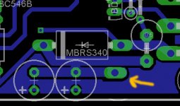
Are R13 and R10 OK? Sometimes the color code is ambiguous. Is the track to R13 OK?
There can be a small difference in dissipation, because the voltage of the zeners will never equal exactly the supply voltage.It seems just one of them much hotter. That one is Q6. Q5 is gentle.
But the difference should be minor, unless the zeners are shorted or have the incorrect voltage.
You can check the collector voltages wrt the negative rail: they should be broadly similar.
Normally, they dissipate 350mW each, which is sufficient to raise the case temperature ~75°C above ambient.
You can thus expect 100°C case, that's perfectly safe and normal.
If there is a large difference between Q5 and Q6, and it is not caused by a difference in voltage, you should try to find why the collector currents are dissimilar.
It probably has a relation with the other anomaly, perhaps a solder bridge in the driver or output region, an incorrect resistor value, a wrongly inserted transistor or something similar.
All the symptoms put together look very, very suspect.
Last edited:
I'm just arrived.
Yes, they are ok.
My supply voltage is 30V. I measured 31.5V one zener to other.
Q6 is -0.60V Q5 is around -7V (yes, seven).
Replacing input pairs doesn't help. Also, dc-offset is same even shortcut to ground or not. I'm investigating.
Thank you for great support.
That is fishy: the BD140's dissipate very similar quiescent power, and if there is a difference, it is necessary to find the cause.
Are R13 and R10 OK? Sometimes the color code is ambiguous. Is the track to R13 OK?
Yes, they are ok.
There can be a small difference in dissipation, because the voltage of the zeners will never equal exactly the supply voltage.
But the difference should be minor, unless the zeners are shorted or have the incorrect voltage.
My supply voltage is 30V. I measured 31.5V one zener to other.
You can check the collector voltages wrt the negative rail: they should be broadly similar.
Q6 is -0.60V Q5 is around -7V (yes, seven).
If there is a large difference between Q5 and Q6, and it is not caused by a difference in voltage, you should try to find why the collector currents are dissimilar.
It probably has a relation with the other anomaly, perhaps a solder bridge in the driver or output region, an incorrect resistor value, a wrongly inserted transistor or something similar.
All the symptoms put together look very, very suspect.
Replacing input pairs doesn't help. Also, dc-offset is same even shortcut to ground or not. I'm investigating.
Thank you for great support.
Yes, they are ok.
No! You hit the target on first shot Elvee..After tracking more carefully, I saw that R13 and R12 are reversed . I just replaced them,and it seems Bd140s ok now.
Still investigating.
Last edited:
DC-offset dropped to 15mV. I will work on this later. But collector voltages on Q6 and Q5 didn't get closed. Q6 is -0.6V, Q5 is dancing around -6.8 -7.3V, not stable. I made two pcbs and both of them have same issue. Q6 is not hot as like previously mentioned but still hotter than Q5.
@powerflux:
15R and 56R on bottom are reversed on silkscreen. Also, you can push them a bit front side due to opening room for driver heatsinks. You can flip 1R and 0.5R in safe. There is enough room.
Bottom side decoupling capacitor's pads different. Upper ones seem good.
You can avoid first bypass cap each side (most left ones) and you can use their pin as supply pad. If you go with this, current will flow through these caps in optimal way. I have modified pdf in this manner. I will post some pics soon.
DC-offset dropped to 15mV. I will work on this later. But collector voltages on Q6 and Q5 didn't get closed. Q6 is -0.6V, Q5 is dancing around -6.8 -7.3V, not stable. I made two pcbs and both of them have same issue. Q6 is not hot as like previously mentioned but still hotter than Q5.
That is not a problem, and anyway the supply is not regulated, meaning that at high output powers, the difference will change (increase further).
The zener's only role is to decrease the dissipation in Q5 and equalize crudely Q5/Q6, but reasonable differences like yours are perfectly acceptable, and have no impact whatsoever on the sonic qualities.
The output offset is also normal, if you want better (not required), you have to match the input transistors. You can also choose suffix -C to minimize offset/bias currents.
Thank you Elvee.. I soldered female pin headers in place of input pairs for easy try out.
I meant decoupling caps of course..
@powerflux:
You can avoid first bypass cap each side (most left ones) ...
I meant decoupling caps of course..
@powerflux:
15R and 56R on bottom are reversed on silkscreen. Also, you can push them a bit front side due to opening room for driver heatsinks. You can flip 1R and 0.5R in safe. There is enough room.
Bottom side decoupling capacitor's pads different. Upper ones seem good.
You can avoid first bypass cap each side (most left ones) and you can use their pin as supply pad. If you go with this, current will flow through these caps in optimal way. I have modified pdf in this manner. I will post some pics soon.
you are correct, my apologies. i've swapped those values on silkscreen and i've also moved the resistors to give the BD's more space for future revisions. you can now put one sheet of +/- 1.5mm aluminium across the board and mount both BD's to it. they're "in-line" i've got the feeling there will be more recommendations so i won't attach this subversion at the moment, only a screenshot.

just make shure to first mount BD's and "cooling-sheet" before surrounding components.
however, i don't understand what you mean by different pads. negative pin is octagon, positive is round.
Last edited:
you are correct, my apologies. Swapped values on silkscreen and i've also moved the resistors to give the BD's more space for future revisions.
i've got the feeling there will be more recommendations so i won't attach this subversion at the moment.
however, i don't understand what you mean by different pads. negative pin is octagon, positive is round.
I expected each side pin as same. If there is a design rule, then it's not a big of deal. But my recommendation regarding using first caps as supply pad should be a good improvement.
EDIT: I depicted on last last revision. Also, wire jumper's pads too small for etch and drill.
@Elvee
Dc-offset is under 1mV now..It seems putting volume pot after input cap causing varying input impedance thus producing weird offset readings. My bad.
Attachments
Last edited:
You are really lucky this time: getting less than one mV spread on two randomly chosen discrete transistors is rather unusual.@Elvee
Dc-offset is under 1mV now..It seems putting volume pot after input cap causing varying input impedance thus producing weird offset readings. My bad.

I didn't get better than 5mV on any my Circlophones, but of course, to play the game fairly, I duly constrained myself to use only suffix-less, unsorted, unmatched BC's.
The input filter has been carefully designed to offer an equal impedance to the bias currents, and when you disturb all that, it is normal to see things deviate.
Anyway, it is always a bad idea to rely on the wiper of a potentiometer to conduct a bias current. At the very least, you risk unpleasant noises when you manoeuvre it.
You are really lucky this time: getting less than one mV spread on two randomly chosen discrete transistors is rather unusual.
I didn't get better than 5mV on any my Circlophones, but of course, to play the game fairly, I duly constrained myself to use only suffix-less, unsorted, unmatched BC's.
The input filter has been carefully designed to offer an equal impedance to the bias currents, and when you disturb all that, it is normal to see things deviate.
Anyway, it is always a bad idea to rely on the wiper of a potentiometer to conduct a bias current. At the very least, you risk unpleasant noises when you manoeuvre it.
After putting potentiometer in right place, offset dropped into this unexpected level. I got this value with pair of exact hfe match 2sa970's (hfe=353) and matched 470R's and 10K's and other symmetrical things as well. I'm not bothering to measure things before populate. BD140's are even same. Actually, I wasn't aiming minimum offset while populating, it was just a habit of symmetry. I think that the matter is topology of Circlophone. Everything is symmetrical from input to output.
Last edited:
That's cheating!!!I got this value with pair of exact hfe match 2sa970's (hfe=353)
It eliminates the offset current, and the Vbe-Hfe correlation does the rest.
It is no surprise you end up with 1mV.
That's cheating!!!
It eliminates the offset current, and the Vbe-Hfe correlation does the rest.
It is no surprise you end up with 1mV.
Actually it is far below of 1mV
BTW, I'm trying to figure out why new PCBs didn't operate as silent as previous wakibaki's.. wakibaki's has performed freaking dead silent without any extra effort. Could wider ground plane be the reason?
Last edited:
What kind of noise do you hear?BTW, I'm trying to figure out why new PCBs didn't operate as silent as previous wakibaki's.. wakibaki's has performed freaking dead silent without any extra effort. Could wider ground plane be the reason?
What kind of noise do you hear?
It is not a typical hiss. Looks like some environmental HF noise interfering my gear. If I disconnect my source (linear supplied soundcard) I can hear a very distorted radio channel which is a known issue due to big antennas near my house. If source connected, noise level is quite gentle but audible nearby speakers. My speakers are 100db.
Last edited:
Is the input filter R19 C5 properly implemented, on board?
Did you try with the input shorted?
Does the board serve as relay point for various grounds?
Did you try to disconnect everything that has a common ground with the amp?
Try disconnecting the speaker, and replace it with headphones having minimal wiring length. (no signal obviously, and be very careful not to blow your eardrum with a sudden bad contact or similar).
Does the hiss change when you move your hand near the board?
Is the input filter R19 C5 properly implemented, on board?
I respected pcb as is. It seems pcb layout and schematic a bit different if we concern about input signal current. C5 is behind of R19 in pcb but, C5 is the most close one to input pair in original schematic. Please take a look there.
I didn't use C5 in wakibaki's pcb. I couldn't have opportunity for re-setup wakibaki's pcb yet. It seems things will be clear if I do same setup again for a fair comparison.
Did you try with the input shorted?
Yes, it is worst as like as input disconnected.
Does the board serve as relay point for various grounds?
It seems No.
Did you try to disconnect everything that has a common ground with the amp?
Yes, it is no effect.
Try disconnecting the speaker, and replace it with headphones having minimal wiring length. (no signal obviously, and be very careful not to blow your eardrum with a sudden bad contact or similar).
Does the hiss change when you move your hand near the board?
My speakers are very are close to setup and I did it without headphone. No effect. If I grab and move input and speaker cable, noise and radio signal raises somewhere that what looks like playing with an antenna. I used bigger polystyrene type cap at zobel (C7) in previous pcb but small mkp type in latest pcb. I haven't altered it yet.
Last edited:
- Home
- Amplifiers
- Solid State
- ♫♪ My little cheap Circlophone© ♫♪